Scaricare la presentazione
La presentazione è in caricamento. Aspetta per favore

1
Dispositivi programmabili

2
Dispositivi programmabili
Sono dispositivi hardware (chip) che mettono a disposizione elementi logici piu’ o meno complessi che possono essere opportunamente interconnessi secondo diverse configurazioni in funzione delle specifiche di progetto Dispongono di Componenti logici (porte logiche, Flip-Flop, Buffer) Linee di connessione Sistemi di inetrconnessione (Multiplexer, connessioni) Porte di I/O Tipologie di Circuiti Programmabili PLA, PAL, ROM. CPLD FPGA
 che mettono a disposizione elementi logici piu’ o meno complessi che possono essere opportunamente interconnessi secondo diverse configurazioni in funzione delle specifiche di progetto. Dispongono di. Componenti logici (porte logiche, Flip-Flop, Buffer) Linee di connessione. Sistemi di inetrconnessione (Multiplexer, connessioni) Porte di I/O. Tipologie di Circuiti Programmabili. PLA, PAL, ROM. CPLD. FPGA.")
3
Dispositivi Programmabili
I diversi dispositivi possono essere classificati in base a diversi aspetti: Modalita’ di programmazione programmabili a maschera (MPGA) programmabili una volta (Fuse o Antifuse) riprogrammabili (EEPROM, SRAM) riconfigurabili (SRAM) Connessioni Globali Locali e distribuite
 programmabili una volta (Fuse o Antifuse) riprogrammabili (EEPROM, SRAM) riconfigurabili (SRAM) Connessioni. Globali. Locali e distribuite.")
4
Modalita’ di programmazione
FUSE Le connessioni tra linee sono inizialmente tutte attive In fase di programmazione si disattivano permanentemente le connessioni inutili ANTIFUSE Le connessioni tra linee sono inizialmente tutte inattive In fase di programmazione si attivano permanentemente le connessioni utili EEPROM le connessioni inizialmente sono tutte inattive In fase di programmazione si possono attivare o disattivare elettricamente in modo non distruttivo Lo stato viene mantenuto anche in assenza di alimentazione

5
Modalita’ di programmazione
SRAM le connessioni inizialmente sono tutte inattive In fase di programmazione si possono attivare o disattivare elettricamente in modo non distruttivo Lo stato NON viene mantenuto in assenza di alimentazione Maggiore velocita’ di programmazione rispetto la tecnologia EEPROM In base alla tecnologia la programmazione puo’ avvenire: Durante la fase non operativa del dispositivo (riprogrammabile) Durante la fase operativa del dispositivo (riconfigurabile) Si interviene separatamente su varie parti del dispositivo
 Durante la fase operativa del dispositivo (riconfigurabile) Si interviene separatamente su varie parti del dispositivo.")
6
Fuse Le linee del dispositivo sono in origine tutte connesse
La programmazione consiste nel “BRUCIARE” (fuse) alcune connessioni in modo tale da mantenere solo quelle necessarie La programmazione avviene mediante una tensione piu’ elevata di quella di normale funzionamento
 alcune connessioni in modo tale da mantenere solo quelle necessarie. La programmazione avviene mediante una tensione piu’ elevata di quella di normale funzionamento.")
7
Antifuse Le linee del dispositivo sono in origine tutte disconnesse
La programmazione consiste nel “CREARE” (antifuse) le connessioni necessarie La programmazione avviene mediante una tensione piu’ elevata di quella di normale funzionamento
 le connessioni necessarie. La programmazione avviene mediante una tensione piu’ elevata di quella di normale funzionamento.")
8
EEPROM Le linee del dispositivo sono in origine tutte disconnesse
La programmazione consiste nel “DEPOSITARE” una carica sul gate flottante del transistor in modo da mandarlo in conduzione La cancellazione puo’ avvenire elettricamente o tramite esposizione a raggi UV

9
SRAM (RAM statica) Le linee del dispositivo sono in origine tutte disconnesse La programmazione consiste nel “MEMORIZZARE” un valore logico (‘0’ o ‘1’) in una cella di RAM Statica
 in una cella di RAM Statica.")
10
Connessioni Connessione Globale Connessione locale
Linea che attraversa buona parte del dispositivo e condivisa da molti elementi logici Elevati ritardi Puo’ essere pilotata da un solo elemento logico (scarsa flessibilita’) Connessione locale Linea che attraversa una parte ridotta del dispositivo ed e’ condivisa da pochi elementi ritardi piu’ contenuti elevata flessibilita’
 Connessione locale. Linea che attraversa una parte ridotta del dispositivo ed e’ condivisa da pochi elementi. ritardi piu’ contenuti. elevata flessibilita’")
11
Connessioni Le connessioni globali sono caratteristiche dei
Dispositivi logici a due livelli: PAL, PLA, ROM CPLD (Complex Programmable Logic Device) Le connessioni locali sono caratteristiche degli FPGA (Field Programmable Gate Array)
 Le connessioni locali sono caratteristiche degli. FPGA (Field Programmable Gate Array)")
12
Logiche programmabili a 2 livelli
Sono usate per realizzare funzioni logiche a due livelli NOTA1: qualunque funzione combinatoria puo’ essere espressa come somma di termini minimi NOTA2: si possono realizzare funzioni a piu’ livelli sfuttando la retroazione Dispongono di: Un numero di ingressi fissato (Buffer di Ingresso) Un piano di AND (per realizzare i termini minimi) Un piano di OR (per realizzare le somme) Un numero di uscite fissato (Buffer di Uscita)
 Un piano di AND (per realizzare i termini minimi) Un piano di OR (per realizzare le somme) Un numero di uscite fissato (Buffer di Uscita)")
13
Logiche programmabili a due livelli
Vi sono tre tipi principali PLA (Programmable Logic Array) Piano AND programmabile Implementa solo i termini minimi necessari Piano OR programmabile PAL (Programmable Array Logic) Piano OR fissato Impone un vincolo sul numero di termini minimi che la funzione contiene ROM (Read Only Memory) Piano AND fissato Implementa tutti i possibili termini minimi (DECODER) Piano OR programmabile
 Piano AND programmabile. Implementa solo i termini minimi necessari. Piano OR programmabile. PAL (Programmable Array Logic) Piano OR fissato. Impone un vincolo sul numero di termini minimi che la funzione contiene. ROM (Read Only Memory) Piano AND fissato. Implementa tutti i possibili termini minimi (DECODER) Piano OR programmabile.")
14
Programmable Logic Array (PLA)
Consente di realizzare qualunque funzione logica Questa e’ espressa in somme di implicanti

15
Programmable Logic Array (PLA)
Schema logico di una PLA Esempio con 3 ingressi e due uscite (non programmata)
")
16
Programmable Logic Array (PLA)
ESEMPIO1: Realizzazione delle funzioni f1 = ab + ac’ + a’b’c f2 = ab + ac + a’b’c Prodotti p1 = ab p2 = ac p3 = ac’ p4 = a’b’c Somme f1 = p1 + p3 + p4 f2 = p1 + p2 + p4 Formato PLA: 11- 10 1-0 10 001 10 11- 01 1-1 01 001 01

17
Programmable Logic Array (PLA)
")
18
Programmable Logic Array (PLA)
")
19
Programmable Logic Array (PLA)
")
20
Programmable Logic Array (PLA)
")
21
Programmable Array Logic (PAL)
Piano di AND programmabile e piano OR fissato Consente di implementare somme di prodotti Vi puo’ essere un limite sul numero massimo di prodotti che possono concorrere nella realizzazione di una funzione

22
Programmable Array Logic (PAL)
Schema logico di una PAL Esempio di PAL a 3 ingressi e 2 uscite (non programmata)
")
23
Read Only Memory (ROM) Puo’ essere realizzata con un piano di AND fisso e completo e con un piano di OR programmabile In pratica implementa m funzioni a n ingressi ad una configuarzione d’ingresso (INDIRIZZO) viene associata una configurazione d’uscita (PAROLA) Il piano AND agisce da DECODIFICATORE degli indirizzi
 viene associata una configurazione d’uscita (PAROLA) Il piano AND agisce da DECODIFICATORE degli indirizzi.")
24
Read Only Memory (ROM) Piano AND (decodificatore degli indirizzi)
realizza tutti i possibili termini minimi per ogni configurazione d’ingresso attiva una ed una sola linea d’uscita

25
Read Only Memory (ROM) Schema logico del piano AND
 Schema logico del piano AND")
26
Read Only Memory (ROM) Schema logico di una ROM
Esempio di una ROM a 3 ingressi e 4 uscite (non programmata)
")
27
Read Only Memory (ROM) Esempio:
dalla tabella di verita’ della funzione a piu’ uscite

28
Read Only Memory (ROM) Realizzazione della funzione
 Realizzazione della funzione")
29
PLA e PAL avanzate PLA e PAL consentono di realizzare solo reti combinatorie a due livelli Questo limite puo’ essere superato Introducendo una rete di reazione permette di implementare reti combinatorie a piu’ di due livelli Introducendo elementi di memoria (Flip-Flop) permette di implementare macchine sequenziali (sincrone)
 permette di implementare macchine sequenziali (sincrone)")
30
PLA e PAL avanzate Esempio di implementazione di una rete combinatoria a piu’ livelli grazie alla retroazione

31
PLA e PAL avanzate Esempio: realizzazione

32
PLA e PAL avanzate L’aggiunta di elementi di memoria in uscita possono ulteriormente ampliare le prestazioni del dispositivo

33
CPLD Complex Programmable Logic Device
Sono la logica evoluzione di PAL e PLA Sono caratterizzati da: Connessioni globali Logica Concentrata Rispetto PAL e PLA Sono piu’ complessi e hanno dimensioni maggiori Consentono di ottenere prestazioni piu’ elevate

34
Programming Controller
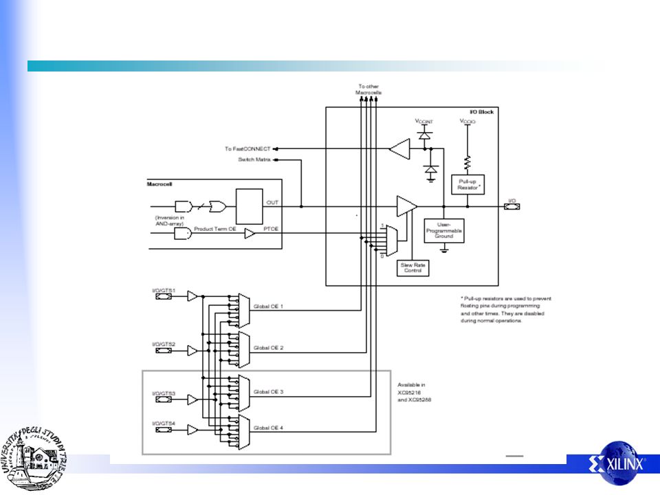
CPLD - XC9500 Architecture 3 In-System Programming Controller JTAG Controller JTAG Port 5 volt in-system programmable (ISP) CPLDs 5 ns pin-to-pin 36 to 288 macrocells (6400 gates) Industry’s best pin-locking architecture 10,000 program/erase cycles Complete IEEE JTAG capability I/O Function Block 1 I/O Function Block 2 I/O I/O Blocks FastCONNECT Switch Matrix I/O Global Clocks Function Block 3 3 Global Set/Reset 1 Function Block 4 Global Tri-States 2 or 4
 CPLDs. 5 ns pin-to-pin. 36 to 288 macrocells (6400 gates) Industry’s best pin-locking architecture. 10,000 program/erase cycles. Complete IEEE JTAG capability. I/O. Function. Block 1. I/O. Function. Block 2. I/O. I/O. Blocks. FastCONNECT. Switch Matrix. I/O. Global Clocks. Function. Block Global Set/Reset. 1. Function. Block 4. Global Tri-States. 2 or 4.")
35
XC9500 Function Block Each function block is like a 36V18 ! To
FastCONNECT From 2 or 4 3 Global Tri-State Clocks I/O 36 Product- Term Allocator Macrocell 1 AND Array Macrocell 18 Each function block is like a 36V18 !

36
Struttura della macrocella
Struttura XC9500 Struttura della macrocella

37
Struttura del “product term allocator”
Struttura XC9500 Struttura del “product term allocator”

38
Struttura XC9500 Possibilita’ di collegamento offerte dal “product term allocator”

39
Struttura XC9500 Possibilita’ di collegamento offerte dal “product term allocator”

40
Linee globali di clock, set, reset
Struttura XC9500 Linee globali di clock, set, reset

41
Struttura XC9500 Cella di I/O

42
XC9500 Product Family 9536 9572 95108 95144 95216 95288 Macrocells 36
Usable Gates 800 1600 2400 3200 4800 6400 tPD (ns) 5 7.5 7.5 7.5 10 10 Registers 36 72 108 144 216 288 Max I/O 34 72 108 133 166 192 Packages VQ44 PC44 PC44 PC84 TQ100 PQ100 PC84 TQ100 PQ100 PQ160 PQ100 PQ160 HQ208 BG352 PQ160 HQ208 BG352
 Registers Max I/O Packages. VQ44. PC44. PC44. PC84. TQ100. PQ100. PC84. TQ100. PQ100. PQ160. PQ100. PQ160. HQ208. BG352. PQ160. HQ208. BG352.")
43
XC Q e A Q: E’ possibile realizzare tramite CPLD XC9500 la seguente architettura?

44
XC Q e A Q: E’ possibile realizzare tramite CPLD XC9500 la seguente architettura? A: NO con una CPLD si possono realizzare solo circuiti DIGITALI

45
XC Q e A Q: E’ possibile realizzare tramite CPLD XC9500 la seguente funzione, ossia un predeterminato RITARDO asincrono ? In Out RIT = 20ns

46
XC Q e A Q: E’ possibile realizzare tramite CPLD XC9500 la seguente funzione, ossia un predeterminato RITARDO asincrono ? In Out RIT = 20ns A: NO: non vi e’ alcun modo o alcun elemento che possa realizzare questa funzione. Nota1: nei circuiti digitali il ritardo e’ una conseguenza (indesiderata) della struttura stessa del circuito e non un parametro da soddisfare Nota2: Un elemento di ritardo e’ tuttavia realizzabile in modo SINCRONO
 della struttura stessa del circuito e non un parametro da soddisfare. Nota2: Un elemento di ritardo e’ tuttavia realizzabile in modo SINCRONO.")
47
XC Q e A Q: E’ possibile realizzare tramite CPLD XC9500 la seguente funzione logica (gli ingressi e le uscite siano collegati direttamente ai pin di I/O del dispositivo)?
")
48
XC Q e A Q: E’ possibile realizzare tramite CPLD XC9500 la seguente funzione logica (gli ingressi e le uscite siano collegati direttamente ai pin di I/O del dispositivo)? A: NO: Non esiste alcun collegamento diretto tra i pin e la logica interna, ma bisogna passare attraverso ai buffer di I/O (il tool di sviluppo corregge automaticamente questo tipo di errore)
 A: NO: Non esiste alcun collegamento diretto tra i pin e la logica interna, ma bisogna passare attraverso ai buffer di I/O. (il tool di sviluppo corregge automaticamente questo tipo di errore)")
50
XC Q e A Q: E’ possibile realizzare tramite CPLD XC9500 la seguente funzione (una logica pilota altre logiche struttando un bus tri-state) Logic 2 Logic 3 Logic 1

51
XC Q e A Q: E’ possibile realizzare tramite CPLD XC9500 la seguente funzione (una logica pilota altre logiche struttando un bus tri-state) Logic 2 Logic 3 Logic 1 A: NO ! Gli unici buffer tri-state del dispositivo sono disponibili nei blocchi di I/O e pertanto non possono essere usati per pilotare logiche interne al dispositivo stesso! (un eventuale loop dal pin di uscita dovrebbe passare attraverso un buffer di ingresso che ne annullerebbe l’effetto

52
FPGA: Introduzione Le FPGA (Field Programmable Gate Array) sono dispositivi programmabili costituiti da una matrice di componenti logici collegabili tra loro Complex Programmable Logic Device (CPLD) Field-Programmable Gate Array (FPGA) Architecture PAL/22V10-like Gate array-like More Combinational More Registers + RAM Density Low-to-medium Medium-to-high 0.5-10K logic gates 1K to 3.2M system gates Performance Predictable timing Application dependent Up to 250 MHz today Up to 200 MHz today Interconnect “Crossbar Switch” Incremental
 sono dispositivi programmabili costituiti da una matrice di componenti logici collegabili tra loro. Complex Programmable Logic Device (CPLD) Field-Programmable Gate Array (FPGA) Architecture PAL/22V10-like Gate array-like. More Combinational More Registers + RAM. Density Low-to-medium Medium-to-high K logic gates 1K to 3.2M system gates. Performance Predictable timing Application dependent. Up to 250 MHz today Up to 200 MHz today. Interconnect Crossbar Switch Incremental.")
53
FPGA Le FPGA mettono a disposizione dell’utente
Componenti logici (CLB - Slice) costituiti da logica, piccole memorie, flip-flop, buffer, multiplexer. Linee di connessione sia locali (corte) che distribuite (lunghe) Matrici di inter-connessione per collegare varie line tra loro e da queste ai blocchi logigi Blocchi di I/O particolari blocchi logici dedicati all’I/O provvedono Buffer, protezioni, Fan-out, resistenze di pull-up e pull-down, adattatori d’impedenza, … Blocchi particolari memorie, moltiplicatori, PLL, decodificatori, …
 costituiti da. logica, piccole memorie, flip-flop, buffer, multiplexer. Linee di connessione. sia locali (corte) che distribuite (lunghe) Matrici di inter-connessione. per collegare varie line tra loro e da queste ai blocchi logigi. Blocchi di I/O. particolari blocchi logici dedicati all’I/O provvedono Buffer, protezioni, Fan-out, resistenze di pull-up e pull-down, adattatori d’impedenza, … Blocchi particolari. memorie, moltiplicatori, PLL, decodificatori, …")
54
FPGA Pregi e difetti: Estremamente versatili
Elevata complessita’ computazionale Piu’ lente di CPLD e ASIC Costo elevato per singolo componente (ma esistono famiglie particolarmente economiche) Costo del prototipo ridotto “Time to market” molto ridotto Possibilita’ di “upgrade” del circuito (anche a distanza) Ottime per la realizzazione di prototipi, (ma si usano sempre di piu’ anche negli elevati volumi di fabbricazione) Capacita’ di supportare sistemi interni (embedded systems)
 Costo del prototipo ridotto. Time to market molto ridotto. Possibilita’ di upgrade del circuito (anche a distanza) Ottime per la realizzazione di prototipi, (ma si usano sempre di piu’ anche negli elevati volumi di fabbricazione) Capacita’ di supportare sistemi interni (embedded systems)")
55
XC4000 Architecture and Features

56
XC4000 Architecture Programmable Interconnect I/O Blocks (IOBs)
Configurable Logic Blocks (CLBs)
")
57
XC4000E/X Configurable Logic Blocks
D Q SD RD EC S/R Control 1 F' G' H' DIN H Func. Gen. G F G4 G3 G2 G1 F4 F3 F2 F1 C4 C1 C2 C3 K YQ Y XQ X H1 DIN S/R EC 2 Four-input function generators (Look Up Tables) - 16x1 RAM or Logic function 2 Registers - Each can be configured as Flip Flop or Latch - Independent clock polarity - Synchronous and asynchronous Set/Reset
 - 16x1 RAM or. Logic function. 2 Registers. - Each can be. configured as Flip. Flop or Latch. - Independent. clock polarity. - Synchronous and. asynchronous. Set/Reset.")
58
Look Up Tables Combinatorial Logic is stored in 16x1 SRAM Look Up Tables (LUTs) in a CLB Example: Look Up Table 4-bit address Combinatorial Logic A B C D Z A B C D Z 4 (2 ) 2 = 64K ! Capacity is limited by number of inputs, not complexity Choose to use each function generator as 4 input logic (LUT) or as high speed sync.dual port RAM G Func. Gen. G4 G3 G2 G1 WE
 2. = 64K ! Capacity is limited by number of inputs, not complexity. Choose to use each function generator as 4 input logic (LUT) or as high speed sync.dual port RAM. G. Func. Gen. G4. G3. G2. G1. WE.")
59
XC4000X I/O Block Diagram Shaded areas are not included in XC4000E family.

60
Xilinx FPGA Routing 1) Fast Direct Interconnect - CLB to CLB
2) General Purpose Interconnect - Uses switch matrix 3) Double Lines 4) Long Lines Segmented across chip Global clocks, lowest skew 2 Tri-states per CLB for busses CLB Switch Matrix
 General Purpose Interconnect - Uses switch matrix. 3) Double Lines. 4) Long Lines. Segmented across chip. Global clocks, lowest skew. 2 Tri-states per CLB for busses. CLB. Switch. Matrix.")
61
What’s Really In that Chip?
Programmable Interconnect Points, PIPs (White) Switch Matrix Routed Wires (Blue) Direct Interconnect (Green) CLB (Red) Long Lines (Purple)
 Switch. Matrix. Routed Wires (Blue) Direct. Interconnect. (Green) CLB. (Red) Long Lines. (Purple)")
62
Spartan-II Architecture and Features

63
Xilinx Your Programmable Logic Solution
Features Virtex-II Spartan-IIE Let’s look at the current offering of FPGA and CPLD families from Xilinx. Xilinx has multiple product families. From the low power market leader CPLD, CoolRunner family to the advanced FPGA Families of Virtex. The Spartan-IIE FPGA and XC9500XL CPLD Families are targeted for the low cost, high volume system level designs that require up to 200K system gates. The CoolRunner CPLD family addresses the high performance, low power market segment. The Virtex/E/EM families are designed to meet the needs of high performance, high level design solutions. The focus of the winning edge is Spartan-IIE and XC9500XL families. FPGAs SRAM-based Feature Rich Low Cost FPGAs SRAM-based Feature Rich High Performance CPLDs Low Power 10K K M Density (System Gates)
")
64
Features Plentiful logic and memory resources Flexible I/O interfaces
15K to 200K system gates (up to 5,292 logic cells) Up to 57 Kb block RAM storage Flexible I/O interfaces From 86 to 284 I/Os 16 signal standards Advanced 0.25/0.22um 6-Layer Metal Process High performance System frequency as high as 200 MHz Spartan FPGAs provide the low cost and high feature content required to be used in consumer electronics applications. Advanced Clock Control with 4 Dedicated DLLs Unlimited Re-programmability Fully PCI Compliant
 Up to 57 Kb block RAM storage. Flexible I/O interfaces. From 86 to 284 I/Os. 16 signal standards. Advanced 0.25/0.22um 6-Layer Metal Process. High performance. System frequency as high as 200 MHz. Spartan FPGAs provide the low cost and high feature content required to be used in consumer electronics applications. Advanced Clock Control with 4 Dedicated DLLs. Unlimited Re-programmability. Fully PCI Compliant.")
65
Spartan-II Top-level Architecture
Configurable logic blocks Implement logic here! I/O blocks Communicate with other chips Choose from 16 signal standards Block RAM On-chip memory for higher performance Now we will look at the details of the architecture. Each of these sections will be examined in more detail later in the presentation.

66
Spartan-II Top-level Architecture
Clocks and delay locked loops Synchronize to clock on and off chip Rich interconnect resources Three-state internal buses Power down mode Lower quiescent power

67
CLB Structure F5IN CIN CLK CE COUT D Q CK S R EC O G4 G3 G2 G1 Look-Up Table Carry & Control Logic YB Y F4 F3 F2 F1 XB X BY SR SLICE The configurable logic block (CLB) contains two slices. Each slice contains two 4-input look-up tables (LUT), carry & control logic and two registers. There are two 3-state buffers associated with each CLB, that can be accessed by all the outputs of a CLB. Xilinx is the only major FPGA vendor that provides dedicated resources for on-chip 3-state bussing. This feature can increase the performance and lower the CLB utilization for wide multiplex functions. The Xilinx internal bus can also be extended off chip. Each slice has 2 LUT-FF pairs with associated carry logic Two 3-state buffers (BUFT) associated with each CLB, accessible by all CLB outputs
 contains two slices. Each slice contains two 4-input look-up tables (LUT), carry & control logic and two registers. There are two 3-state buffers associated with each CLB, that can be accessed by all the outputs of a CLB. Xilinx is the only major FPGA vendor that provides dedicated resources for on-chip 3-state bussing. This feature can increase the performance and lower the CLB utilization for wide multiplex functions. The Xilinx internal bus can also be extended off chip. Each slice has 2 LUT-FF pairs with associated carry logic. Two 3-state buffers (BUFT) associated with each CLB, accessible by all CLB outputs.")
68
Sommatore veloce Xilinx

69
CLB Slice (Simplified)
1 CLB holds 2 slices Each slice contains two sets of the following: Four-input LUT Any 4-input logic function Or 16-bit x 1 RAM Or 16-bit shift register The FPGA is made up of an array of Configurable Logic Blocks (CLBs), and each CLB is made up of two slices, and each slice has two Look-Up Tables (LUTs) and 2 flip-flops.
, and each CLB is made up of two slices, and each slice has two Look-Up Tables (LUTs) and 2 flip-flops.")
70
CLB Slice (cont’d) Each slice contains two sets of the following:
Carry & control Fast arithmetic logic Multiplier logic Multiplexer logic Storage element Latch or flip-flop Set and reset True or inverted inputs Sync. or async. control

71
Four-Input LUT = Implements combinatorial logic Truth Table
Any 4-input logic function Cascaded for wide-input functions Truth Table LUT = 4-input logic function C D Z A B LUT is also known as function generator. It can be used to form any function of its four inputs. The software automatically cascades these LUTs to build wide input logic functions.

72
Distributed RAM = or = or CLB LUT configurable as Distributed RAM
RAM16X1S LUT D = WE WCLK CLB LUT configurable as Distributed RAM A LUT equals 16x1 RAM Implements Single and Dual-Ports Cascade LUTs to increase RAM size Synchronous write Synchronous/Asynchronous read Accompanying flip-flops used for synchronous read A0 O A1 A2 A3 RAM32X1S D WE WCLK A0 O A1 LUT A2 A3 A4 or RAM16X2S O1 D0 WE WCLK A0 A1 A2 A3 D1 O0 = RAM16X1D D LUT WE When the CLB LUT is configured as memory, it can implement 16x1 synchronous RAM. One LUT can implement 16x1 Single-Port RAM. Two LUTs are used to implement 16x1 dual port RAM. The LUTs can be cascaded for desired memory depth and width. The write operation is synchronous. The read operation is asynchronous and can be made synchronous by using the accompanying flip flops of the CLB LUT. The distributed ram is compact and fast which makes it ideal for small ram based functions. WCLK or A0 SPO A1 A2 A3 DPRA0 DPO DPRA1 DPRA2 DPRA3

73
Shift Register = Each LUT can be configured as shift register
Serial in, serial out Dynamically addressable delay up to 16 cycles For programmable pipeline Cascade for greater cycle delays Use CLB flip-flops to add depth Use for programmable clock delay D Q CE LUT IN CLK DEPTH[3:0] OUT = The LUT can be configured as a shift register (serial in, serial out) with bit width programmable from 1 to 16. For example, DEPTH[3:0] = 0010(binary) means that the shift register is 3-bit wide. In the simplest case, a 16 bit shift register can be implemented in a LUT, eliminating the need for 16 flip flops, and also eliminating extra routing resources that would have been lowered the performance otherwise.
 with bit width programmable from 1 to 16. For example, DEPTH[3:0] = 0010(binary) means that the shift register is 3-bit wide. In the simplest case, a 16 bit shift register can be implemented in a LUT, eliminating the need for 16 flip flops, and also eliminating extra routing resources that would have been lowered the performance otherwise.")
74
Shift Register Register-rich FPGA
64 Operation A 4 Cycles 8 Cycles Operation B 3 Cycles Operation C 12 Cycles 9-Cycle imbalance Register-rich FPGA Allows for addition of pipeline stages to increase throughput Data paths must be balanced to keep desired functionality In this example, there is a cycle imbalance, which must be fixed. Let’s think of how the shift register can fix the imbalanced cycles. As seen from the slide, the logic will be off by nine clock cycles.

75
Shift Register LUT as shift register Increase overall register count
12 Cycles 64 Operation A 4 Cycles 8 Cycles Operation B 3 Cycles Operation C Paths statically balanced 9 Cycles Pipeline LUT as shift register Used to add pipeline stages Increase overall register count 16 bit shift register per LUT 64 bit shift register per CLB The shift register functionality (Operation D) can be used in the path to obtain valid output by adding nine additional cycles. Alternatively, this design would have required additional logic and a counter to hold the data until the right time.
 can be used in the path to obtain valid output by adding nine additional cycles. Alternatively, this design would have required additional logic and a counter to hold the data until the right time.")
76
CLB Arithmetic Logic Dedicated carry logic
Provides high performance for counters & arithmetic functions Discrete XOR component for single level sum completion Two separate carry chains in CLB allow for 3 operand functions Can also be used to cascade LUTs for wide-input logic functions Single-level Sum You will see two carry chains present in a CLB. The discrete exclusive-OR gates (XOR) are used to compute sum of inputs in one logic level. Note that the Altera FLEX 10K and ACEX 1K families have only one carry chain in their LAB.
 are used to compute sum of inputs in one logic level. Note that the Altera FLEX 10K and ACEX 1K families have only one carry chain in their LAB.")
77
3 Operand Adder Function
COUT Look-Up Table SLICE0 CIN O Carry & Control Logic SLICE1 CLB B1 B0 A1 A0 C1 C0 SUM1 SUM0 PARTIAL0 PARTIAL1 Two carry chains are used to implement SUM = A + B + C function within a CLB. First carry chain is used to perform partial sum, A +B. The second carry chain is used to perform the sum of PARTIAL and C. Note that the synthesis tools may not be able to infer both the carry chains in the CLB. In that case, you will need to place the logic using the floorplanner before implementing the design. In the above example, two carry chains within a CLB would give higher performance as opposed to Altera’s solution with just one carry chain in their Logic Array Block(LAB). A, B, C are two-bits wide SUM = A + B + C or PARTIAL + C, where PARTIAL = A + B Implementation First 2-operand sum ‘A+B’ is performed in Slice 0 Second 2-operand sum ‘PARTIAL + C’ is performed in Slice 1 Fast local feedback connection within the CLB Very small delay for on PARTIAL
. A, B, C are two-bits wide. SUM = A + B + C or PARTIAL + C, where PARTIAL = A + B. Implementation. First 2-operand sum ‘A+B’ is performed in Slice 0. Second 2-operand sum ‘PARTIAL + C’ is performed in Slice 1. Fast local feedback connection within the CLB. Very small delay for on PARTIAL.")
78
Sommatore a 4 bits Carry Out Overflow Carry In

79
Dedicated Expansion Multiplexers
MUXF5 combines 2 LUTs to form 4x1 multiplexer Or any 5-input function MUXF6 combines 2 slices to form 8x1 multiplexer Or any 6-input function CLB MUXF6 Slice LUT MUXF5 Special logic in the CLB allows logic expansion beyond just using the lookup tables.

80
Memory Bandwidth and Flexibility
Spartan-II on-chip SelectRAM+TM memory Large FIFOs Packet Buffers Video Line Buffers Cache Tag Memory Deep/Wide megabytes SDRAM ZBTRAM SSRAM SGRAM External RAM bytes 16x1 DSP Coefficients Small FIFOs Shallow/Wide Distributed RAM 4Kx1 2Kx2 1Kx4 512x8 256x16 Three types of memory are supported - small distributed RAM in the LUTs, large block RAM, or very large external RAM. Block RAM kilobytes 200 MHz Memory Continuum Highest performance FPGA memory system

81
Block RAM Provides 4K Bits Each
Dual read/write ports, each with: Independent clock, R/W, and enable Independently configurable data width from 4Kx1 to 256x16 Spartan-II Dual-R/W Port Block RAM Port A Port B W R Data Flow Spartan-II A to B Yes B to A Yes A to A Yes B to B Yes

82
Local Routing Interconnect among LUTs, FFs, GRM
The local routing provides: -connect logic within the CLB -path to connect to horizontally adjacent CLBs Interconnect among LUTs, FFs, GRM CLB feedback path for connections to LUTs in same CLB Direct path between horizontally adjacent CLBs

83
General Purpose Routing
INTERNAL BUSSES Internal 3-state Bus Long lines and Global lines Buffered Hex lines Single-length lines DIRECT CONNECTION Direct connections Xilinx provides automatic place and route tools efficiently use these routing The designers do not need to worry about this process. 24 single-length lines Route GRM signals to adjacent GRMs in 4 directions 96 buffered hex lines Route GRM signals to another GRMs six blocks away in each of the four directions 12 buffered Long lines Routing across top and bottom, left and right

84
Internal Three-state Buses

85
Routing Summary Vector-based routing Core-friendly architecture
Predictable routing delays independent of device size and routing direction Core-friendly architecture Quick Place and Route times Design to system at 100,000 gates per minute Easier re-routing Internal 3-state bussing Eliminates bus routing contention Improves density and performance CLB Array The Spartan-IIE family has vector based routing structure that provides routing delays independent of direction and device size. This feature is very useful for IP cores because it gives predictable timing for the IP; regardless of number of IPs, their placement and the device being used. The routing structure is abundant in the Spartan-IIE family. This in turn helps reduce the compile times. For example, a design of 100K gates targeting a Spartan-IIE can be routed in 1 minute with the release of the 3.1i software. Future version of the software should reduce these times even further. Xilinx is the only major FPGA vendor that provides dedicated resources for on-chip 3-state bussing. This feature can increase the performance and lower the CLB utilization for wide multiplexor functions. The Altera FPGAs do not have these resources. To emulate this functionality in their FPGAs would require extra LUTs with multiple levels of logic. The Xilinx internal bus can also be extended off chip.

86
Clock distribution Nets
High speed Low skew 4 distribution nets 4 dedicated input PADS 4 dedicated Global buffers with inputs or from clock pad from internal signal

87
System Clock Management
Mirror clock for board distribution DLL1 DLL2 De-skew clocks 4 low-skew global clocks System Clocks Convert clock to different I/O standards using SelectI/O™ DLL3 DLL4 Multiply Divide Shift Spartan-IIE includes powerful chip and board level clock management with DLLs. DLLs are the 100% digital implementation of the old analog PLLs. Spartan-IIE contains 4 DLLs in each device. The DLLs perform the following functions: - Remove on-chip as well as off-chip clock delays (de-skew) - Clock multiplication, division and phase shift - Clock duplication for distribution to other chips on the system board - Clock output conversion to a different IO standard e.g. SSTL, using SelectI/O feature of the Spartan-IIE family. XAPP174 on the Xilinx web explains about DLLs with further details. The Altera FLEX 10KE and ACEX 1K families provide only one PLL, only on the fastest speed grade as an option at added cost. Delay Lock Loops (DLLs) Lower Board Costs
 - Clock multiplication, division and phase shift. - Clock duplication for distribution to other chips on the system board. - Clock output conversion to a different IO standard e.g. SSTL, using SelectI/O feature of the Spartan-IIE family. XAPP174 on the Xilinx web explains about DLLs with further details. The Altera FLEX 10KE and ACEX 1K families provide only one PLL, only on the fastest speed grade as an option at added cost. Delay Lock Loops (DLLs) Lower Board Costs.")
88
DLL Capabilities Easy clock duplication
System clock distribution Cleans and reconditions incoming clock Quick and easy frequency adjustment Single crystal easily generates multiple clocks Faster state machine utilizing different clock phases Excellent for advance memory types De-skew incoming clock Generate fast setup and hold time or fast clock-to-outs Clock Mirror duplicates incoming clock and performs system synchronization. Multiple and Divide functions allow simple frequency adjustments for distribution through out the board. By using inexpensive crystals, clock frequencies can by multiplied internally to the FPGA reducing board EMI. Clock Phase Shift provides coarse phase shifts of 0, 90, 180 and 270 degrees. Excellent for the fast clocking of State Machines by utilizing each of the different clock phases. Clock de-skew allows for faster setup, hold and clock-to-out times allowing higher overall system performance. Clock De-skew

89
Generic DLL Operation A DLL inserts delay on the clock net until the clock input rising edge is in phase with the clock feedback rising edge Requires a well-designed clock distribution network: the clock edges arrive simultaneously everywhere in the part Delay CLKIN Phase Delay Control CLKOUT CLKFB Clock Distribution Network DLL inserts a delay until the delayed feedback clock aligns with the input clock. At that point the DLL is locked.

90
Delay-locked Loop Functions
Eliminate clock distribution delay System synchronization (e.g., clock mirrors) Phase-shifted clocks Clock multiplication and division Clean up clocks with 50/50 duty cycle correction Clock lock for internal & external synchronization DLL feedback connected internally or externally Can synchronize configuration to DLL lock
 Phase-shifted clocks. Clock multiplication and division. Clean up clocks with 50/50 duty cycle correction. Clock lock for internal & external synchronization. DLL feedback connected internally or externally. Can synchronize configuration to DLL lock.")
91
Improved Clock-to-out Using DLL
Spartan-II clock-to-out delays reduced over 50% Output standard = LVTTL Fast 16mA (OBUF_F_16) Temp=room, Vdd=2.5V, Vcco=3.3V Waveforms: 1: CLKIN 2: DATA OUT (no DLL) 3: DATA OUT (DLL deskewed) Timing w/o DLL w/ DLL r->r r->f r->r r->f 3.6n 3.5n 1.4n 1.4n A key benefit of the DLL is the ability to “remove” delay from the clock path, and improve the effective clock-to-out delay.
 Temp=room, Vdd=2.5V, Vcco=3.3V. Waveforms: 1: CLKIN. 2: DATA OUT (no DLL) 3: DATA OUT (DLL deskewed) Timing. w/o DLL w/ DLL. r->r r->f r->r r->f. 3.6n 3.5n 1.4n 1.4n. A key benefit of the DLL is the ability to remove delay from the clock path, and improve the effective clock-to-out delay.")
92
DLL Macros Two DLL versions available CLKDLL (low frequency)
Controlled by macro choice CLKDLL (low frequency) Input frequency: 25 MHz to 100 MHz All 6 outputs available CLK0, CLK90, CLK180, CLK270, CLK2X & CLKDV CLKDLLHF (high frequency) Input frequency 60 MHz to 200 MHz 3 outputs available CLK0, CLK180 & CLKDV
 Input frequency: 25 MHz to 100 MHz. All 6 outputs available. CLK0, CLK90, CLK180, CLK270, CLK2X & CLKDV. CLKDLLHF (high frequency) Input frequency 60 MHz to 200 MHz. 3 outputs available. CLK0, CLK180 & CLKDV.")
93
I/O Block (Simplified)
Registered input, output, 3-state control Programmable slew rate, pull-up, pull-down, keeper and input delay The I/O block features are automatically used according to the design entered into the development system.

94
IOBs Organized As Independent Banks
As many as eight banks on a device Package dependent Each bank can be assigned any of the 16 signal standards

95
Programmable Output Driver
Simultaneous Switching Output Guidelines Significant EMI reduction benefit Programmable driver strength Pull-up and Pull-down drivers can be individually controlled 16 different setting for each 2 slew rate settings

96
System Interfaces -- SelectI/O™
Voltage Standards 2.5V 1.8V 3.3V 1.5V 19 Different Standards Supported! SSTL HSTL CTT High-speed Memory Interfaces Chip-to-Chip Interfaces LVTTL LVCMOS LVPECL LVDS Backplane Interfaces GTL GTL+ AGP PCI BLVDS The Select I/O technology provides a universal I/O translation capability across many voltage levels and signaling standards. This capability is unique in the FPGA world and facilitates easy communication among chip-chip, chip-to-memory and chip-to-backplane applications. Each Select I/O pin can support any standard and each Spartan-IIE FPGA can support multiple standards simultaneously. Up to eight different standards can be supported simultaneously. SelectI/O helps to eliminate the number of translator chips on the board by incorporating industry used standards on the same chip. Traditionally, a bus transceiver chip would have been used to interface the FPGA to other chips such as high speed DDR RAM. Now that the functionality of the transceiver chip is already incorporated into the Spartan-IIE chip, translation chips are no longer needed. Thus the chip count on the board gets reduced, there by saving board space, reducing board costs and improving overall reliability. It is worthy to note that in the past we usually used only LVTTL or LVCMOS as a basic signaling standard. Spartan-IIE still supports these standards. These are the standards usually used in legacy systems to interface to older devices. Note that the Altera FLEX 10KE and ACEX 1K families do NOT support the latest I/O standards. They have only 5 standards, and only one can be used at a given time. Supports multiple voltage and signal standards simultaneously Eliminate costly bus transceivers

97
SelectI/OTM Standards
User I/O Pin VCCO VREF Internal Reference Output Input VCCO defines output voltage The table shows the reference voltage and the output source voltage for various standards. Note that the Altera FLEX 10KE and ACEX 1K families do NOT support the latest I/O standards. They have only five standards, and only one can be used at a given time. VREF defines input threshold reference voltage Available as user I/O when using internal reference

98
Spartan-II As Center for Signal Translation
SDRAM SSTL GTL+ LVTTL LVCMOS CTT SRAM HSTL Chip to Chip LVTTL, LVCMOS Chip to Memory SSTL2-I, SSTL2-II, SSTL3-I, SSTL3-II, HSTL-I, HSTL-III, HSTL-IV, CTT Chip to Backplane PCI33-5V, PCI33-3.3V, GTL, GTL+, AGP No external translators are necessary when using the Spartan-II family. Allows support for future standards!

99
Partial Reconfiguration
Frame by frame reconfiguration supported while device is running Routing changes affect device operation Re-initializing a block RAM requires stopping all access in that column Can dynamically load the required logic at a given time Minimizes cost further by time-multiplexing the logic resources

100
Power-down Mode Controlled by single power down pin
All inputs blocked, appear low internally All outputs disabled All register states preserved Power-down status pin Synchronous wake up 100 uA typical A dedicated Power Down pin helps conserve the power resources.

101
Configuration Modes There are four ways to program a Spartan-II FPGA
The user can choose the configuration mode that best suits the particular application. There are four ways to program a Spartan-II FPGA

102
Spartan-II Family Overview
The XC2S200 was recently added to extend the family to 200,000 system gates.

103
Spartan-II Architecture Summary
Delivers all the key requirements for ASIC replacement 200,000 gates 200 MHz Flexible I/O interfaces On-chip distributed and block RAM Clock management Low power Complete development system support

Presentazioni simili


 Problemi classici di IPC Scheduling Processi e thread in Unix Processi.>")


 relazionale client/server.>")


>")

