Scaricare la presentazione
La presentazione è in caricamento. Aspetta per favore

1
4D-MPET 4D-MPET: un rivelatore innovativo per I tomografi PET di futura generazione M. G. Bisogni Dipartimento di Fisica e INFN Pisa Pisa, 15/6/2010

2
Outline PET Basics PET detectors The DASIPM project The 4D-MPET proposal

3
PET Basics

4
PET Physics Event generation: annihilation Detection principle: time coincidence energy threshold to reject Compton scattering

6
PET advantages Coincidence detection at 180 Higher sensitivity Better signal/noise ratio Easier attenuation correction Sum of two paths inside =body thickness More physiologic radiopharmaceuticals (C11, N-13, O-15, F18)
")
7
Limits to the PET spatial resolution *Derenzo & Moses, "Critical instrumentation issues for resolution <2mm, high sensitivity brain PET", in Quantification of Brain Function, Tracer Kinetics & Image Analysis in Brain PET, ed. Uemura et al, Elsevier, 1993, pp. 25-40.

8
PET spatial resolution 8 Non collinearity Positron Range Crystal sizeCoding 1.2:Degradation due to reconstruction d:Crystal pitch b:Coding error (range: 0-2 mm) D:Detector separation r:effective source size (including positron range) p:Parallax error *Derenzo & Moses, "Critical instrumentation issues for resolution <2mm, high sensitivity brain PET", in Quantification of Brain Function, Tracer Kinetics & Image Analysis in Brain PET, ed. Uemura et al, Elsevier, 1993, pp. 25-40. Parallax error

9
Parallax error Depth Of Interaction DOI The “depth of interaction (DOI)” information helps to reduce the a parallax error that results in a spatial resolution degradation in the radial direction of the field of view
 information helps to reduce the a parallax error that results in a spatial resolution degradation in the radial direction of the field of view")
10
Not only resolution the importance of counts 10 One of the main requirements for a PET tomograph is the sensitivity. In PET systems resolution and sensitivity are a trade- off 50 000 counts100 000 counts200 000 counts 500 000 counts1 million counts2 million counts 4.8mm 6.4mm 11.1mm 12.7 mm 7.9 mm 9.5mm

11
Time Of Flight (TOF)-PET 11 PET traditional The probability for the event to be located along the LOR is uniform t1t1 t2t2 t 2 -t 1 PET Time-of-Flight The most likelihood position is in the center of the error distribution TOF-PET systems exploit the time difference between the two emitted photons to better locate the annihilation position. The limit in the annihilation point location is mainly due to the error in the time difference measurement, namely the time resolution t of the coincidence system Time resolution is used by the reconstruction algorithm to locate the annihilation point x ( x =c t/2)
.")
12
Back project one line Back project all linesReconstructed image TOF Principles of TOF PET

13
TOF reconstruction = sensitivity amplification or noise reduction D is patient “diameter”, t is time resolution of TOF PET scanner * estimate based on uniform cylindrical object and analytical reconstruction t (ps) x (cm) G NEC (D=40cm) G SNR (D=40cm) 3004.58.93.0 40066.72.6 5007.55.32.3 60094.42.1 Principles of TOF PET
 x (cm) G NEC (D=40cm) G SNR (D=40cm) Principles of TOF PET")
14
non-TOF, 3i21s (120 sec) TOF, 2i14s (60 sec) TOF reconstruction produces comparable image with ½ of the counts (590 ps reconstruction kernel) Advantages of TOF PET: Counts amplifier
 TOF, 2i14s (60 sec) TOF reconstruction produces comparable image with ½ of the counts (590 ps reconstruction kernel) Advantages of TOF PET: Counts amplifier")
15
Past and present of TOF PET scanners: Siemens mCT TOF PET

16
The Block Detector 1984-1985 Burnham, Brownell and colleagues at MGH developed a technique where scintillators were placed on a circular lightguide with photomultipliers placed on the opposite side of the lightguide. Charlie Burnham demonstrated that by taking the ratio of two adjacent photomultiplier signals, the scintillator that detected the gamma ray could be identified. Mike Casey and Ronald Nutt, from CTI, introduce the "Block“ detector that was conceived as a means to simplify the Burnham detector and to make it easier to manufacture. Almost all dedicated tomographs built since 1985 have used some forms of the Block detector. This invention has made possible high-resolution PET tomographs at a much-reduced cost. The block detector Scintillators placed on a circular light guide with photomultipliers on opposite side of light guide.

17
Principle of Operation 17 In a block detector, a 2D array of crystals are attached to 4 PMTs. Usually the array will be cut from a single crystal and the cuts filled with light-reflecting material. When a photon is incident on one of the crystals, the resultant light is shared by all 4 PMTs. Information on the position of the detecting crystal may be obtained from the PMT outputs by calculating the following ratios and comparing them to pre-set values: where A, B, C and D are the fractional amounts of light detected by each PMT

18
Still PMTs? 18 Avalanche Photodiodes (APDs) Silicon Photomultipliers(SiPMs) o Geiger-mode APD Since more than 80 years, the PMT is the photodetector of choice to convert scintillation photons into electrical signals in most of the applications related to the radiation detection. This is due to its high gain, low noise and fast response Research is now moving to solid state photodetectors that show the following advantages with respect to PMTs: Compactness High quantum efficiency (to provide an energy resolution comparable to PMTs) Insensitivity to magnetic fields( PET/MRI )
 Silicon Photomultipliers(SiPMs) o Geiger-mode APD Since more than 80 years, the PMT is the photodetector of choice to convert scintillation photons into electrical signals in most of the applications related to the radiation detection. This is due to its high gain, low noise and fast response Research is now moving to solid state photodetectors that show the following advantages with respect to PMTs: Compactness High quantum efficiency (to provide an energy resolution comparable to PMTs) Insensitivity to magnetic fields( PET/MRI ).")
19
Multimodality Imaging Hybrid systems: the future commercial PET/CT systems available solid state technology allow the devlopment of PET-MRI systems Siemens MADPET II Hamamatsu S8550 LSO 4x8 pixel

20
PET + MR: Semantic Dementia 20 MR [ 18 F]FDG Fused
![PET + MR: Semantic Dementia 20 MR [ 18 F]FDG Fused](http://images.slideplayer.it/33/10505695/slides/slide_20.jpg "PET + MR: Semantic Dementia 20 MR [ 18 F]FDG Fused")
21
Technical Challenges in PET/MR 21 Interference on PET (photomultiplier and electronics) Static magnetic field Electromagnetic interference from RF and gradients Interference on MR (homogeneity and gradients) Electromagnetic radiation from PET electronics Maintaining magnetic field homogeneity Eddy currents Susceptibility artifacts General Challenges Space Environmental factors (temperature, vibration…) Cost PET attenuation correction via MR data is a challenge!
 Static magnetic field Electromagnetic interference from RF and gradients Interference on MR (homogeneity and gradients) Electromagnetic radiation from PET electronics Maintaining magnetic field homogeneity Eddy currents Susceptibility artifacts General Challenges Space Environmental factors (temperature, vibration…) Cost PET attenuation correction via MR data is a challenge!")
22
Brain PET/MRI 22 Ring of LSO detectors inserted in a 3T MR tomograph Simultaneous PET and MR data acquisition Courtesy of Berndt Pichler, University of Tubingen PET Insert

23
23 MR-PET Head Insert New integrated Detector Block Prototype PET Head-Insert gantry phantom head coil RF shield Courtesy of Berndt Pichler, University of Tubingen

24
The SiPM solution? 24 p + substrate π epilayer p high-electric field multiplication region n + cathode h +V GM oxide 4 µm e-e- hole SiPM: Multicell Avalanche Photodiode working in limited Geiger mode - 2D array of microcells: structures in a common bulk. - Vbias > Vbreakdown: high field in multiplication region - Microcells work in Geiger mode: the signal is independent of the particle energy - The SiPM output is the sum of the signals produced in all microcells fired. SOLID STATE PHOTODETECTOR High gain(~ 10 6 ) low bias voltage (~ 50V) Linear response with the photon flux (for Nfot <<Ncell) PDE dark noise(1-2 MHz/mm 2 @ 1 fotone)
 low bias voltage (~ 50V) Linear response with the photon flux (for Nfot <<Ncell) PDE dark noise(1-2 MHz/mm 1 fotone).")
26
Pisa, 2 Dicembre 2009 C. Piemonte 26 The SiPM tile 32.7mm Fill factor ~ 84% (not including SiPM FF) Flat surface for crystal mounting 700 working arrays delivered for the preclinical system PCB design and mounting at Uni. Heidelberg and Philips 500 m
 Flat surface for crystal mounting 700 working arrays delivered for the preclinical system PCB design and mounting at Uni. Heidelberg and Philips 500 m.")
27
The INFN DASiPM2 Project Sezioni di: Bari, Bologna, Pisa, Perugia,Trento Progetto DASiPM (Development and Application of SiPM) INFN-group V - 2005 Progetto SiPM Sviluppo di rivelatori SiPM INFN-group V - 2006 Produzione e caratterizzazione di SiPM ottimizzati nella regione 400-500 nm Produzione di matrici di SiPM Progetto DASiPM2 (Development and Application of SiPM) INFN-group V - 2007 SiPM Applications: Medical Imaging: small animal PET demonstrator Astroparticle: TOF SipM module High Energy Physics: tracking calorimeter w scintillating fibers
 INFN-group V Progetto SiPM Sviluppo di rivelatori SiPM INFN-group V Produzione e caratterizzazione di SiPM ottimizzati nella regione nm Produzione di matrici di SiPM Progetto DASiPM2 (Development and Application of SiPM) INFN-group V SiPM Applications: Medical Imaging: small animal PET demonstrator Astroparticle: TOF SipM module High Energy Physics: tracking calorimeter w scintillating fibers")
28
Characterization 28 Collaboration with FBK- irst (Trento, Italy), that has been developing SiPMs since 2005: First detectors - Single SiPMs (2006) First matrices 2x2 (2007) First matrices 4x4 (2008) First matrices 8x8 (2009) Breakdown voltage VB ~ 30V, very good uniformity. Gain: ~10 6 Linear for a few volts over V BD. Related to the recharge of the diode capacitance C D from V BD to V BIAS during the avalanche quenching. G=(VBIAS-VB) x C D /q Dark rate : 1-3 MHz at 1-2 photoelectron (p.e.) level, ~kHz at 3-4 p.e (room temperature). Not a concern for PET applications.
 x C D /q Dark rate : 1-3 MHz at 1-2 photoelectron (p.e.) level, ~kHz at 3-4 p.e (room temperature). Not a concern for PET applications..")
29
Intrinsic timing 29 Intrinsic timing measured at s.p.e level: 60 ps ( ) for blue light at 4V overvoltage. SiPM illuminated with a pulsed laser with 60 fs pulse width and 12.34 ns period, with less than 100 fs jitter. Two wavelengths used: = 400 7 nm and = 800 15 nm. Time difference between contiguous pulses is determined. The timing decreases with the number of photoelectrons as 1/√(Npe) 20 ps at 15 photoelectrons. λ = 800 nm λ = 400 nm — contribution from noise and method (not subtracted) [eye guide] [G. Collazuol et al., VCI 2007, NIM A 2007, A581, 461-464] λ = 400 nm at 4 V overvoltage [fit as 1/√(N pe )]
 20 ps at 15 photoelectrons. λ = 800 nm λ = 400 nm — contribution from noise and method (not subtracted) [eye guide] [G. Collazuol et al., VCI 2007, NIM A 2007, A581, ] λ = 400 nm at 4 V overvoltage [fit as 1/√(N pe )].")
30
New Ca co-doped LSO:Ce crystals LSO:Ce shows limitations as Afterglow that limits the high counting rate applications Non-linearity especially under 100 keV The newly developed LSO:Ce crystals co-doped with calcium divalent cations showed higher light output and faster light pulses The most recent studies also showed that co-doping of LSO:Ce with Ca substantially reduces afterglow intensity. C. L. Melcher and J. S. Schweitzer, “Cerium-doped lutetium oxyorthosilicate: A fast, efficient new scintillator,” IEEE Trans. Nucl. Sci., vol. 39, no. 4, pp. 502–505, Aug. 1992. C. L. Melcher et al, “Effects of Ca Co-Doping on the Scintillation Properties of LSO:Ce,” IEEE Trans. Nucl. Sci., vol. 55, no. 3, pp. 1178–1182, Jun.2008. C. L. Melcher et al. “Effects of calcium co-doping on charge traps in LSO:Ce,” in Proc. IEEE Nuclear Science Symp. Conf. Rec., Oct. 26–Nov. 3 2007, vol. 4, pp. 2476–2479, 2007.

31
Time resolution

32
Energy Resolution

33
Tests of SIPM in a MR system (MRI) in collaboration with the Wolfson Brain Imaging Center, Cambridge, UK 33 S.p.e and 22 Na energy spectra acquired with gradients off (black line) and on (red line). No real difference is appreciated in the data. Differences in photopeak position is due to temperature changes in the magnet apparent change in gain due to changes in breakdown voltage gradients off gradients on gradients off gradients on [ R.C.Hawkes,et al. 2007 IEEE NSS-MIC, Honolulu, USA, October 28-November 3, 2007: M18-118. ]

34
Different geometries 34 Matrices 16 elements (4x4) 1mm 1x1mm 2 2x2mm 2 3x3mm 2 (3600 cells) 4x4mm 2 (6400 cells) Different geometry,size,microcell size and GF. 4 mm 40x40 m 2 => GF 44% 50x50 m 2 => GF 50% 100x100 m 2 => GF 76% circular 1.3cm

35
Matrices for INFN-DaSiPM2 project (2009) 35 1.3cm 8x8 matrix 1.5mm element pitch 625 (50 m x 50 m) cells read-out both on one or two sides
 cm 8x8 matrix 1.5mm element pitch 625 (50 m x 50 m) cells read-out both on one or two sides")
36
Static Characterization 36 IV plot of the 64 elements of the matrix IV plot of the 64 elements of the matrix Breakdown voltage over the entire wafer surface Breakdown voltage over the entire wafer surface

37
37 Setup probe station INFN Perugia

38
PG1=W9C2; PG2=W9C4

39
IV CURVE after gluing and bonding before gluing and bonding

40
Spectroscopic characterization

41
Matrix 8x8: first 22 Na spectrum 41 E/E = 17% FWHM G. Llosa, IEEE-NSS-MIC 2009 LYSO black slab 10 x 10 x 5 mm^3 Put on top of the SiPM matrix V over-br =4V E/E =14%

42
Spatial Resolution 42 Reconstructed position with center of gravity algorithm. The spatial resolution is about 1 mm FWHM as obtained with a standard center of gravity algorithm.

43
Position Reconstruction 43

44
Maximum Likelihood Method

45
Large detector gain wide dynamic range required ! Example: 300 hit micro-cells, gain=10 6, Q TOT =48pC voltage swing on a 5pF integration capacitance Q TOT /C = 9.6V !! Avalanche breakdown very fast signal, accurate timing feasible wideband electronics Front-end electronic noise: negligible contribution Current-mode approach Front-end electronics for SiPM C. Marzocca, IEEE-NSS-MIC 2009

46
Variable gain integrator Gain: 1V/pC, 0.5V/pC, 0.33V/pC f = 200ns Output voltage range: 0.3V ÷ 2.8V Current buffer scaling factor M=10 Architecture of the analog channel

47
Architecture of BASIC

48
Main features of the chip Three operating modes: write configuration, read configuration and acquisition Two acquisition modes: “sparse read-out” and “serial read-out” Standard cell read-out logic All the channels share the same Vrif (8-bit DAC) and I_th (4-bit DAC) 8 bit successive approximation ADC from a library Fast-OR circuit operating in current mode, to increase the speed of operation Layout of the prototype (3.2 x 2.2 mm 2, CMOS 0.35 m)
 and I_th (4-bit DAC) 8 bit successive approximation ADC from a library Fast-OR circuit operating in current mode, to increase the speed of operation Layout of the prototype (3.2 x 2.2 mm 2, CMOS 0.35 m)")
49
Read-out procedure for the test chip A)An event activates the SRQ bus (by default at Hi-Z) B)FPGA gives a time-stamp to the event and takes control of the SRQ bus during the read-out procedure C)SRQ, in its active state, is used to “freeze” the content of the trigger registers (no more trigger are accepted) D)FPGA waits the time needed by the PDs to reach the peak and sends the CLOCK signal to the ASICs F)The read-out logic starts the A/D conversions and sends the results to FPGA on the DATA_i pad G)When all the conversions have been completed, FPGA releases the SRQ bus and sends a RESET signal SRQ CHIP DATA CLOCK FPGA DATA_0 CLOCK SRQ RESET Package SMD
An event activates the SRQ bus (by default at Hi-Z) B)FPGA gives a time-stamp to the event and takes control of the SRQ bus during the read-out procedure C)SRQ, in its active state, is used to freeze the content of the trigger registers (no more trigger are accepted) D)FPGA waits the time needed by the PDs to reach the peak and sends the CLOCK signal to the ASICs F)The read-out logic starts the A/D conversions and sends the results to FPGA on the DATA_i pad G)When all the conversions have been completed, FPGA releases the SRQ bus and sends a RESET signal SRQ CHIP DATA CLOCK FPGA DATA_0 CLOCK SRQ RESET Package SMD")
50
Measurements: injection capacitance Peak detector output as a function of the input voltage step amplitude Overall charge to voltage gain very close to the expected one (M*C F ) -1 Equivalent input noise charge 50fC ( out =5mV @ C F =1pF) corresponding to about 1/3 microcell of a SiPM with a 10 6 gain Max dynamic range 70pC @ C F =3pF (1% linearity error) C inj =10pF, M=10 CFCF 1pF2pF3pF Expect. Gain 2.01.00.67 Meas. Gain 2.080.990.68

51
Measurements: LYSO Scintillator + SiPM Counts Energy (keV)
")
52
DASiPM2_DAQ System architecture

53
DASiPM2_DAQ System overview DAQ Boards Motherboard

54
4D-MPET Proposal L'obiettivo principale di questo progetto e' lo sviluppo di un modulo PET 4D di nuova generazione, ad altissime prestazioni, che si candida come possibile successore dell'attuale "block detector". Questo modulo, facilmente ottimizzabile per diverse applicazioni dell' imaging nucleare, fornirà informazioni molto accurate sulla posizione dell'evento in 3 dimensioni e un segnale di timing mantenendo al tempo stesso una elevata efficienza intrinseca. Il design del modulo si basa sull'uso dicristalli continui di scintillatore in combinazione con al silicio ad alta granularità, ottimizzabile per ciascuna applicazione, che permette ladeterminazione della posizione con alta precisione, nonché la determinazione della DOI e del tempo di volo (TOF) massimizzando al tempo stesso, l'efficienza dirivelazione. Completamente compatibile con MRI scanner
 massimizzando al tempo stesso, l efficienza dirivelazione. Completamente compatibile con MRI scanner.")
55
1.2 cm Proposed geometry 4.8 cm 1 cm Sipm matrix 8x8 pixels Pitch 1.5 mm Single SiPM 4x4 mm^2 Annihilation gamma Front side Back side

56
Aspetti innovativi Utilizzo di scintillatori continui Utilizzo di LSO:Ce,CaSaranno utilizzati nuovi scintillatori LSO:Ce co-drogati con Calcio (LSO: Ce, Ca). Questo tipo di scintillatore è stato recentemente prodotto e testato, mostrando untempo di decadimento molto breve (30 ns), una maggiore resa di luce, ed una riduzione dell'afterglow. L'uso di questo scintillatore si tradurrà in un ulterioremiglioramento delle prestazioni in termini di timing del modulo rivelatore, che è essenziale per l'implementazione della tecnica TOF negli scanner PET clinici. Utilizzo di SiPMs.L'alto guadagno intrinseco dei SiPMs rispetto agli APD riduce la necessità di sviluppare un'elettronica a basso rumore. Il vantaggio principale e' la possibilita' dipreservare le alte prestazioni temporali del SiPM, riducendo così il rumore e il pile-up degli eventi, e aumentando il rate di acquisizione sostenibile dal rivelatore.Inoltre, l'alto guadagno consente l'implementazione di tecniche TOF per migliorare la sensibilità del modulo rivelatore. I SiPM sono oggi disponibili con dimensionie caratteristiche differenti e sono commercializzati da diversi fornitori. Matrici (2D array) di fotomoltiplicatori al silicio cresciute su un unico substrato (monolitico)e con lettura laterale sono state prodotte dalla FBK-irst, mentre la Hamamatsu e la SensL hanno prodotto e commercializzato matrici costituite da elementiindipendenti. Elettronica di front-end e chip TDC ad alta risoluzioneI circuiti integrati di Front-End ed i TDC devono rispettare le specifiche dettate dai SiPMs e dagli scintillatori utilizzati nelle diverse applicazioni. L'elettronica devequindi essere veloce, affidabile e in grado di lavorare in ambiente di risonanza magnetica (MR) senza interferire con il sistema. Il design degli ASIC presenta diversecaratteristiche innovative essenziali per la lettura adeguata del modulo rivelatore. Un circuito integrato per l'implementazione di un TDC ad alta risoluzione (sigma~100 ps) sarà collegato ai SiPM di grande area presenti sulla superficie di rivelazione frontale e fornirà il tempo di arrivo dei fotoni su ogni testa di rivelazione(TOF) generando quindi il trigger per l'acquisizione di eventi in coincidenza. I chip di Front-End collegati alle matrici di SiPMs poste sul retro dello scintillatore,forniranno la posizione d'impatto e l' energia depositata associate ad ogni evento. Inoltre, essi avranno un sistema di compensazione attiva per correggere levariazioni di guadagno dei SiPM dovute alla variazione della temperatura. Protocolli veloci e flessibili ed interfacce per la distribuzione del segnaleLo sviluppo di protocolli veloci e flessibili per la distribuzione del trigger, del clock, dei segnali di timing e dei controlli da integrare nel chip di front-end e nel TDCrappresenta un ulteriore passo in avanti verso una completa integrazione dei componenti elettronici progettati per la lettura del modulo. Utilizzo di componenti non magnetici e trasmissione dei segnali via link-ottici
, una maggiore resa di luce, ed una riduzione dell afterglow. L uso di questo scintillatore si tradurrà in un ulterioremiglioramento delle prestazioni in termini di timing del modulo rivelatore, che è essenziale per l implementazione della tecnica TOF negli scanner PET clinici. Utilizzo di SiPMs.L alto guadagno intrinseco dei SiPMs rispetto agli APD riduce la necessità di sviluppare un elettronica a basso rumore. Il vantaggio principale e la possibilita dipreservare le alte prestazioni temporali del SiPM, riducendo così il rumore e il pile-up degli eventi, e aumentando il rate di acquisizione sostenibile dal rivelatore.Inoltre, l alto guadagno consente l implementazione di tecniche TOF per migliorare la sensibilità del modulo rivelatore. I SiPM sono oggi disponibili con dimensionie caratteristiche differenti e sono commercializzati da diversi fornitori. Matrici (2D array) di fotomoltiplicatori al silicio cresciute su un unico substrato (monolitico)e con lettura laterale sono state prodotte dalla FBK-irst, mentre la Hamamatsu e la SensL hanno prodotto e commercializzato matrici costituite da elementiindipendenti. Elettronica di front-end e chip TDC ad alta risoluzioneI circuiti integrati di Front-End ed i TDC devono rispettare le specifiche dettate dai SiPMs e dagli scintillatori utilizzati nelle diverse applicazioni. L elettronica devequindi essere veloce, affidabile e in grado di lavorare in ambiente di risonanza magnetica (MR) senza interferire con il sistema. Il design degli ASIC presenta diversecaratteristiche innovative essenziali per la lettura adeguata del modulo rivelatore. Un circuito integrato per l implementazione di un TDC ad alta risoluzione (sigma~100 ps) sarà collegato ai SiPM di grande area presenti sulla superficie di rivelazione frontale e fornirà il tempo di arrivo dei fotoni su ogni testa di rivelazione(TOF) generando quindi il trigger per l acquisizione di eventi in coincidenza. I chip di Front-End collegati alle matrici di SiPMs poste sul retro dello scintillatore,forniranno la posizione d impatto e l energia depositata associate ad ogni evento. Inoltre, essi avranno un sistema di compensazione attiva per correggere levariazioni di guadagno dei SiPM dovute alla variazione della temperatura. Protocolli veloci e flessibili ed interfacce per la distribuzione del segnaleLo sviluppo di protocolli veloci e flessibili per la distribuzione del trigger, del clock, dei segnali di timing e dei controlli da integrare nel chip di front-end e nel TDCrappresenta un ulteriore passo in avanti verso una completa integrazione dei componenti elettronici progettati per la lettura del modulo. Utilizzo di componenti non magnetici e trasmissione dei segnali via link-ottici.")
57
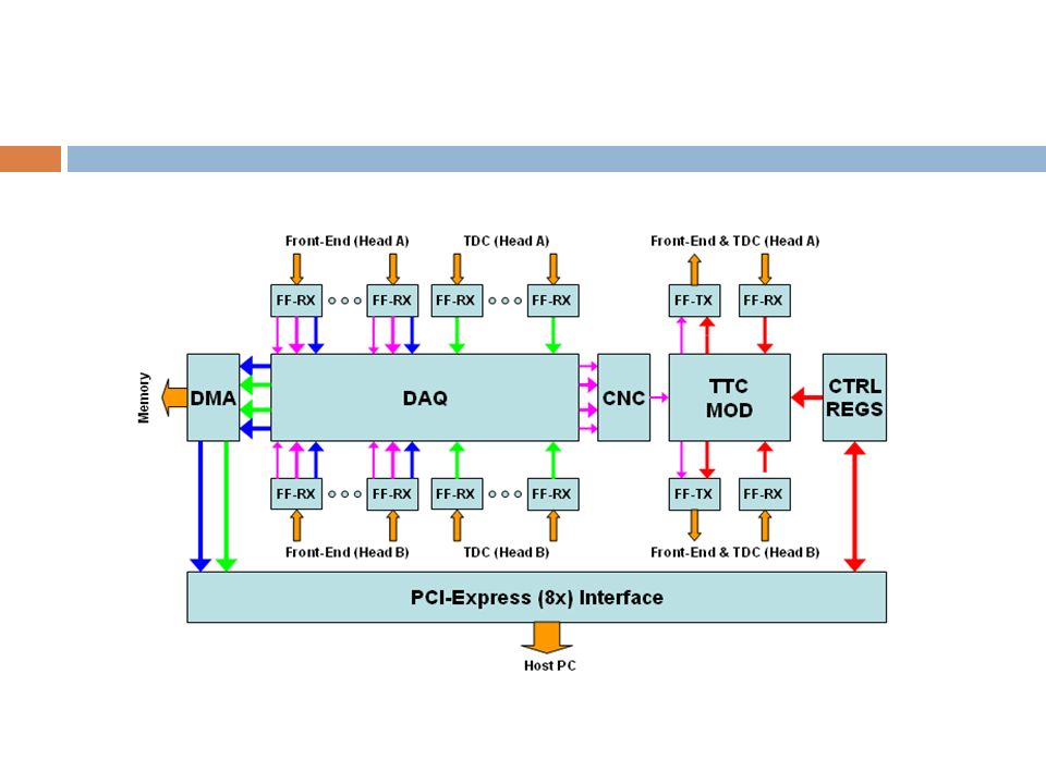
Control, trigger and readout systems for the 4D-MPET detector The control, trigger and readout systems of the 4MDPET will be based on the FF-LYNX protocol and interfaces. The same physical links will be used to distribute Timing, Trigger and Control (TTC) signals and to handle the data acquisition from Front-End circuits on the “Back-Side” (space and energy information and low resolution timing information for the evaluation of the coincidence condition) and from TDC circuits on the “Front-Side” (high resolution timing information for TOF). “Back-Side” has 1024 high resolution SiPMs grouped in 256 clusters (2x2 SiPMs each) corresponding to 256 channels handled by 8 Front-End circuits (32 channels each). The “Front- Side” has 144 low resolution SiPMs handled by 9 TDC circuits (16 channels each). The estimated data rates (events in coincidence) for the Front-End circuits and for the TDC circuits will be 130 Mbps and 65 Mbps respectively. One “single-wire” link (clock and data encoded onto the same serial line, “8b/10b” encoding of the FRM channel) at 400 Mbps (speed = 8xF, frequency of the reference clock cycle = 50 MHz, effective bandwidth 240 Mbps) could handle the readout of each Front-End circuit while 3 TDC circuits could be daisy- chained in a “ring” handled by another “single-wire” link at 400 Mbps. One “double-wire” link (separate clock and data lines) at 200 Mbps (speed = 4xF, effective bandwidth 100 Mbps) could be used to transmit TTC signals to Front-End circuits and TDC circuits connected in a “ring” (redundancy can be optionally introduced to prevent from single component failure). A total number of 15 differential lines could therefore handle one head of the 4DMPET detector: 11 “single-wire” links from Front-End circuits (8) and from TDC circuits (3), 1 “double- wire” TTC link to the detector and 1 “double-wire” TTC link from the detector.
 signals and to handle the data acquisition from Front-End circuits on the Back-Side (space and energy information and low resolution timing information for the evaluation of the coincidence condition) and from TDC circuits on the Front-Side (high resolution timing information for TOF). Back-Side has 1024 high resolution SiPMs grouped in 256 clusters (2x2 SiPMs each) corresponding to 256 channels handled by 8 Front-End circuits (32 channels each). The Front- Side has 144 low resolution SiPMs handled by 9 TDC circuits (16 channels each). The estimated data rates (events in coincidence) for the Front-End circuits and for the TDC circuits will be 130 Mbps and 65 Mbps respectively. One single-wire link (clock and data encoded onto the same serial line, 8b/10b encoding of the FRM channel) at 400 Mbps (speed = 8xF, frequency of the reference clock cycle = 50 MHz, effective bandwidth 240 Mbps) could handle the readout of each Front-End circuit while 3 TDC circuits could be daisy- chained in a ring handled by another single-wire link at 400 Mbps. One double-wire link (separate clock and data lines) at 200 Mbps (speed = 4xF, effective bandwidth 100 Mbps) could be used to transmit TTC signals to Front-End circuits and TDC circuits connected in a ring (redundancy can be optionally introduced to prevent from single component failure). A total number of 15 differential lines could therefore handle one head of the 4DMPET detector: 11 single-wire links from Front-End circuits (8) and from TDC circuits (3), 1 double- wire TTC link to the detector and 1 double-wire TTC link from the detector..")
58
Control, trigger and readout systems The control, trigger and readout systems of the 4MDPET will be based on the FF-LYNX protocol. The same physical links will be used to distribute Timing, Trigger and Control (TTC) signals and to handle the data acquisition from Front-End circuits on the “Back-Side” and from TDC circuits on the “Front-Side”
 signals and to handle the data acquisition from Front-End circuits on the Back-Side and from TDC circuits on the Front-Side .")
60
System View Head 1 FPGA Head 2 PCI- Express(HO ST-PC) MEMORY CLKGEN Few optical connection between the two heads and one motherboard housing an FPGA device that implement the coincidence logic and the interfaces (USB, Ethernet, PCI-Express) to/from the host PC
 MEMORY CLKGEN Few optical connection between the two heads and one motherboard housing an FPGA device that implement the coincidence logic and the interfaces (USB, Ethernet, PCI-Express) to/from the host PC")
61
Integration (“High” resolution option) Top Side (SiPM Matrices) Bottom Side (Front-End ASICs) Vertical vias between top side (SiPM matrices and Bottom side) Horizontal tracks for FF- LYNX Clock and Data lines
 Top Side (SiPM Matrices) Bottom Side (Front-End ASICs) Vertical vias between top side (SiPM matrices and Bottom side) Horizontal tracks for FF- LYNX Clock and Data lines")
62
Detector development 62 Many silicon dies required to cover large surfaces => Electric connections problem

63
Feed Through 63 300-500 µm 1500 µm SIPM sensor 20-150 µm Back contacts: the geometrical constraint is removed

64
Pisa, 2 Dicembre 2009 C. Piemonte 64 Metal ECD: Home-made set up Process difficult to control First prelim. results Hole etching: OK

65
4D-MPET Montecarlo Simulations Simulations of single detector LYSO slab 4.8x4.8x1 cm 3 Coupled to 4x4 matrix of SiPMs Pixel 1.5x1.5 mm 2, other configurations studied (3x3 mm 2 ) Photo Detection Efficiency is forced to be as is shown in the chart, that is the PDE of a SiPM with geom 50% Simulations are made with GAMOS developed at CIEMAT, data analysis and reconstruction with ROOT.
 Photo Detection Efficiency is forced to be as is shown in the chart, that is the PDE of a SiPM with geom 50% Simulations are made with GAMOS developed at CIEMAT, data analysis and reconstruction with ROOT.")
66
Some results Resolution is (at the moment) evaluated with a gaussian fit Pixels of 3x3 mm 2 (red line) instead of 1.5x1.5mm 2 (black line) do not affect the resolution Depth Of Interaction: estimation feasible with detectors at both sides of the LYSO slab. estimated through the asymmetry of the dispertion of the counts distribution on the two sides may be improved with the optimization of the dimensions of the crystal

67
Sezioni INFN partecipanti Pisa (M.G. Bisogni, A. Del Guerra, S. Marcatili, G. Collazuol, N. Marino, L. Fanucci, C. Saponara, R. Roncella, F. Baronti’) Integrazione e caratterizzazione del modulo Elettronica di Read-out ASIC TDC alta risoluzione e protocollo di trasmissione FF-LYNX (DIIET) Bari (F. Corsi, C. Marzocca, M. Foresta, G. Matarrese) ASIC Front-End Perugia (G. Ambrosi, P. Azzarello) Caratterizzazione e test matrici e SiPM singoli Torino (C. Peroni, P.G. Cerello, R. Wheadon, F. Pennazio) Simulazioni Monte Carlo Compatibilita’ magnetica
 Integrazione e caratterizzazione del modulo Elettronica di Read-out ASIC TDC alta risoluzione e protocollo di trasmissione FF-LYNX (DIIET) Bari (F. Corsi, C. Marzocca, M. Foresta, G. Matarrese) ASIC Front-End Perugia (G. Ambrosi, P. Azzarello) Caratterizzazione e test matrici e SiPM singoli Torino (C. Peroni, P.G. Cerello, R. Wheadon, F. Pennazio) Simulazioni Monte Carlo Compatibilita’ magnetica.")
69
Persone Ricercatori % BisogniM.G.80 Del GuerraA.40 MarinoN.70 ErturkS.100 MarcatiliS.100 Assegnista 100 FanucciL.20 SaponaraS.20 RoncellaR.60 BarontiF.60 6.5 FTE/ 10 ric

70
Richieste Finanziarie Richieste 2011 Consumi Componenti Optoelettronici12000 PCB design and production25000 Submission chip25000 Test Tools10000 Inventariabile Stazione CAD+costo quota Cadence6000 PCI Express motherboard9000 PC con 2 bus PCI Express3000 Missioni Interne Riunione collaborazione5000 totale95000

71
Richieste supporto in sezione Servizio AT: 2 MU Servizio Elettronico : progettazione PCB + consulenza firmware FPGA 2 MU Progettazione Meccanica: disegno supporti 1MU Officina Meccanica: realizzazione supporti 1 MU

Presentazioni simili


 0.8 mm pitch M = 2, FoV = 25×25 mm 2 50×50 mm 2 LaBr 3 (Ce) 4 mm thick, 3 mm thick window M = 2, FoV = 25×25 mm 2 50×50 mm 2 CsI(Na)>")
 F. Garibaldi - c.d. s. Roma1, 09-07-2010 PSA SENSITIVITY.>")


.>")

