Scaricare la presentazione
La presentazione è in caricamento. Aspetta per favore

1
Mara Bruzzi INFN, University of Florence, Italy Radiation Damage in Semiconductors Radiation environments and working principles Microscopic radiation damage Impact of Defects on HEP detector properties Macroscopic radiation damage (Si) Material Engineering (Si) Other examples: Dsosimetry and Space solar Cells Conclusions Mara Bruzzi, Danno da radiazione in semiconduttori Scuola Nazionale rivelatori ed elettronica per fisica delle alte energie, astrofisica 12 Aprile 2011, Legnaro, Italy
 Material Engineering (Si) Other examples: Dsosimetry and Space solar Cells Conclusions Mara Bruzzi, Danno da radiazione in semiconduttori Scuola Nazionale rivelatori ed elettronica per fisica delle alte energie, astrofisica 12 Aprile 2011, Legnaro, Italy")
2
Typical working environments for radiation damage EnvironmentRadiation typeTypical exposure Fission reactor0.1-5MeV n5x10 17 m -2 s -1 Fusion reactor0.1-14MeV n8x10 18 m -2 s -1 Space6eV photons10 20 m -2 s -1 10keV-3MeV 5x10 12 m -2 s -1 1MeV-300MeV p4x10 9 m -2 s -1 Ion accelerator15 MeV p6x10 16 m -2 s -1 High energy physics experiments n,p, pions10 14 -10 16 cm -2 radiotherapyX, e, p10kGy Mara Bruzzi, Danno da radiazione in semiconduttori Scuola Nazionale rivelatori ed elettronica per fisica delle alte energie, astrofisica 12 Aprile 2011, Legnaro, Italy

3
High energy Physics experiments at Large Hadron Collider (LHC), CERN, Geneva E cm = 14TeV p-p collision L ~ 10 34 cm -2 s -1 High Energy Physics Experiments Increase of luminosity of LHC up to 10 35 cm -2 s -1 discussed since 2002. Main constraint is the survival of the Si detector tracker to the exceptionally high fluences of fast hadrons. Mara Bruzzi, Danno da radiazione in semiconduttori Scuola Nazionale rivelatori ed elettronica per fisica delle alte energie, astrofisica 12 Aprile 2011, Legnaro, Italy

4
Working principle of a semiconductor detector Insulating > 10 10 cm Ohmic contact Schottky contact n / p semiconductor p + n or n + p junction Mara Bruzzi, Danno da radiazione in semiconduttori Scuola Nazionale rivelatori ed elettronica per fisica delle alte energie, astrofisica 12 Aprile 2011, Legnaro, Italy

5
Selection of semiconductor gap

6
Semiconductor used for detector applications

7
Poisson’s equation Reminder: Reverse biased abrupt p + -n junction Electrical charge density Electrical field strength Electron potential energy effective space charge density depletion voltage Full charge collection only for V B >V dep ! Positive space charge, N eff =[P] (ionized Phosphorus atoms) Mara Bruzzi, Danno da radiazione in semiconduttori Scuola Nazionale rivelatori ed elettronica per fisica delle alte energie, astrofisica 12 Aprile 2011, Legnaro, Italy
 Mara Bruzzi, Danno da radiazione in semiconduttori Scuola Nazionale rivelatori ed elettronica per fisica delle alte energie, astrofisica 12 Aprile 2011, Legnaro, Italy.")
8
The principle application has been to detect the passage of ionising radiation with high spatial resolution and good efficiency. Segmentation → position Depletion depth → efficiency ~80e/h pairs/μm produced by passage of minimum ionising particle, ‘mip’ Pitch ~ 50 m Resolution ~ 5 m Highly segmented silicon detectors have been used in Particle Physics experiments for nearly 30 years. They are the favourite choice for Tracker and Vertex detectors (high resolution, speed, low mass, relatively low cost, and now important, radiation hard) Physics of Micro-strip Silicon Detectors p + in n - Mara Bruzzi, Danno da radiazione in semiconduttori Scuola Nazionale rivelatori ed elettronica per fisica delle alte energie, astrofisica 12 Aprile 2011, Legnaro, Italy
 Physics of Micro-strip Silicon Detectors p + in n - Mara Bruzzi, Danno da radiazione in semiconduttori Scuola Nazionale rivelatori ed elettronica per fisica delle alte energie, astrofisica 12 Aprile 2011, Legnaro, Italy.")
9
Relevant parameters of a detector Leakage Current Capacitance Active region thickness Effective space charge in depleted region Mara Bruzzi, Danno da radiazione in semiconduttori Scuola Nazionale rivelatori ed elettronica per fisica delle alte energie, astrofisica 12 Aprile 2011, Legnaro, Italy

10
Physical parameters and detector requirements Low energy for e-h generation small gap Low leakage current high gap Low full depletion voltage: high resisitivity High Signal / Sensitivity Radiation Hardness High speed High spatial resolution Low Noise High stability High mobility Mara Bruzzi, Danno da radiazione in semiconduttori Scuola Nazionale rivelatori ed elettronica per fisica delle alte energie, astrofisica 12 Aprile 2011, Legnaro, Italy

11
Radiation Damage RoadMap for Semiconductor Devices Radiation induced defects Extended defects or clusters Carrier removal and increase of resistivity Microscopic Damage TrapsRecombination centres Macroscopic Damage Increase of the leakage current Change in N eff and space charge sign - underdepletion Decrease of minority carrier lifetime and diffusion length Midgap Fermi level pinning Decrease of the charge collection, sensitivity and energy conversion efficiency Mara Bruzzi, Danno da radiazione in semiconduttori Scuola Nazionale rivelatori ed elettronica per fisica delle alte energie, astrofisica 12 Aprile 2011, Legnaro, Italy

12
Microscopic Radiation Damage Mara Bruzzi, Danno da radiazione in semiconduttori Scuola Nazionale rivelatori ed elettronica per fisica delle alte energie, astrofisica 12 Aprile 2011, Legnaro, Italy

13
particle Si s Vacancy + Interstitial Point Defects (V-V, V-O.. ) clusters E K > 25 eV E K > 5 keV Frenkel pair V I Simulation of Microscopic Damage Generation of hadronic interactions Transport of the produced heavy recoils Migration of V and I to form stable defects Mara Bruzzi, Danno da radiazione in semiconduttori Scuola Nazionale rivelatori ed elettronica per fisica delle alte energie, astrofisica 12 Aprile 2011, Legnaro, Italy
 clusters E K > 25 eV E K > 5 keV Frenkel pair V I Simulation of Microscopic Damage Generation of hadronic interactions Transport of the produced heavy recoils Migration of V and I to form stable defects Mara Bruzzi, Danno da radiazione in semiconduttori Scuola Nazionale rivelatori ed elettronica per fisica delle alte energie, astrofisica 12 Aprile 2011, Legnaro, Italy.")
14
Character of Frenkel pair depend on relative distance of V and I : if this is not too large ranges the atomic environment deformation of V and I overlap and their coupling is considerable (coupled Frenkel pair). If PKA departed from its site of several lattice constants separated V and I are created: position of energy levels diffusion coefficients maybe appreciably different from those of coupled pair. a: instability zone b: region occupied by coupled Frenkel pairs c: region of separated genetic V and I d: region of isolated V and I Character of the Frenkel Pair While the dimensions of the instability zones in metals are relatively large, the situation in semiconductor is contrary in most cases, the interstitial and vacancy being in neighboring cells, instability zone is restricted to one elementary cell. Mara Bruzzi, Danno da radiazione in semiconduttori Scuola Nazionale rivelatori ed elettronica per fisica delle alte energie, astrofisica 12 Aprile 2011, Legnaro, Italy

15
Proportionality between N t = defect concentration and = particle flux assumed proportional through atomic concentration N 0 and a proportionality coefficient depending on the energy E of the incoming particle : N t defect formation cross section. Cross section can be evaluated e.g. for electrons as: With Z, M atomic number and mass of a crystal atom and m electron mass, E M maximum energy transferred. Thus, (E) tends to zero when E M is lower than the value E d, energy required to separate the Frenkel pair. Non Ionizing Energy Loss (NIEL) and Threshold Energy E d Mara Bruzzi, Danno da radiazione in semiconduttori Scuola Nazionale rivelatori ed elettronica per fisica delle alte energie, astrofisica 12 Aprile 2011, Legnaro, Italy
 tends to zero when E M is lower than the value E d, energy required to separate the Frenkel pair. Non Ionizing Energy Loss (NIEL) and Threshold Energy E d Mara Bruzzi, Danno da radiazione in semiconduttori Scuola Nazionale rivelatori ed elettronica per fisica delle alte energie, astrofisica 12 Aprile 2011, Legnaro, Italy.")
16
Mara Bruzzi, April 11, 2011 Displacement energies E d depend on : (i) Bond strength (ii) Space available for accommodating an interstitial atom in the structure ( may involve electrostatic repulsion for charged interstitials ) (iii) Form of interstitial (iv) Temperature of irradiation Mara Bruzzi, Danno da radiazione in semiconduttori Scuola Nazionale rivelatori ed elettronica per fisica delle alte energie, astrofisica 12 Aprile 2011, Legnaro, Italy
 Bond strength (ii) Space available for accommodating an interstitial atom in the structure ( may involve electrostatic repulsion for charged interstitials ) (iii) Form of interstitial (iv) Temperature of irradiation Mara Bruzzi, Danno da radiazione in semiconduttori Scuola Nazionale rivelatori ed elettronica per fisica delle alte energie, astrofisica 12 Aprile 2011, Legnaro, Italy")
17
Mara Bruzzi, April 11, 2011 Cascades and cluster formation Depending on its initial energy and crystallographic direction the process of collision and displacements initiated by the PKA can involve secondary knock-on atoms in a cascade, giving rise to separate Frenkel pairs and defective clusters composed of several vacancies and interstitials. ▀ Bombarding particle 1 PKA + displaced atom O divacancy Size distribution of vacancy clusters in an Au crystal irradiated with particles of different energies. Mara Bruzzi, Danno da radiazione in semiconduttori Scuola Nazionale rivelatori ed elettronica per fisica delle alte energie, astrofisica 12 Aprile 2011, Legnaro, Italy

18
10 MeV protons 24 GeV/c protons 1 MeV neutrons [Mika Huhtinen NIMA 491(2002) 194] Initial distribution of vacancies in (1 m) 3 after 10 14 particles/cm 2 Vacancy amount and distribution depends on particle kind and energy Neutrons (elastic scattering) –E n > 185 eV for displacement –E n > 35 keV for cluster 60 Co-gammas –Compton Electrons with max. E 1 MeV (no cluster production) Electrons –E e > 255 keV for displacement –E e > 8 MeV for cluster Only point defects point defects & clusters Mainly clusters Mara Bruzzi, Danno da radiazione in semiconduttori Scuola Nazionale rivelatori ed elettronica per fisica delle alte energie, astrofisica 12 Aprile 2011, Legnaro, Italy
![10 MeV protons 24 GeV/c protons 1 MeV neutrons [Mika Huhtinen NIMA 491(2002) 194] Initial distribution of vacancies in (1 m) 3 after particles/cm 2 Vacancy amount and distribution depends on particle kind and energy Neutrons (elastic scattering) –E n > 185 eV for displacement –E n > 35 keV for cluster 60 Co-gammas –Compton Electrons with max.](http://images.slideplayer.it/38/10800420/slides/slide_18.jpg "E 1 MeV (no cluster production) Electrons –E e > 255 keV for displacement –E e > 8 MeV for cluster Only point defects point defects & clusters Mainly clusters Mara Bruzzi, Danno da radiazione in semiconduttori Scuola Nazionale rivelatori ed elettronica per fisica delle alte energie, astrofisica 12 Aprile 2011, Legnaro, Italy.")
19
of a radiation field (or monoenergetic particle) with respect to 1 MeV neutrons E energy of particle D(E) displacement damage cross section for a certain particle at energy E D(1MeV neutrons)=95 MeV·mb (E) energy spectrum of radiation field The integrals are evaluated for the interval [E MIN,E MAX ], being E MIN and E MAX the minimum and maximum cut-off energy values, respectively, and covering all particle types present in the radiation field How to normalize radiation damage from different particles? NIEL - Non Ionizing Energy Loss scaling using hardness factor Mara Bruzzi, Danno da radiazione in semiconduttori Scuola Nazionale rivelatori ed elettronica per fisica delle alte energie, astrofisica 12 Aprile 2011, Legnaro, Italy
![of a radiation field (or monoenergetic particle) with respect to 1 MeV neutrons E energy of particle D(E) displacement damage cross section for a certain particle at energy E D(1MeV neutrons)=95 MeV·mb (E) energy spectrum of radiation field The integrals are evaluated for the interval [E MIN,E MAX ], being E MIN and E MAX the minimum and maximum cut-off energy values, respectively, and covering all particle types present in the radiation field How to normalize radiation damage from different particles.](http://images.slideplayer.it/38/10800420/slides/slide_19.jpg " NIEL - Non Ionizing Energy Loss scaling using hardness factor Mara Bruzzi, Danno da radiazione in semiconduttori Scuola Nazionale rivelatori ed elettronica per fisica delle alte energie, astrofisica 12 Aprile 2011, Legnaro, Italy.")
20
NIEL – Non Ionizing Energy Loss Displacement damage functions Hypothesis: Damage parameters scale with the NIE –Be careful, does not hold for all particles & damage parameters (see later) 1MeV 1 1 MeV neutron equivalent damage Mara Bruzzi, Danno da radiazione in semiconduttori Scuola Nazionale rivelatori ed elettronica per fisica delle alte energie, astrofisica 12 Aprile 2011, Legnaro, Italy
 1MeV 1 1 MeV neutron equivalent damage Mara Bruzzi, Danno da radiazione in semiconduttori Scuola Nazionale rivelatori ed elettronica per fisica delle alte energie, astrofisica 12 Aprile 2011, Legnaro, Italy")
21
- Secondary defect formation in silicon Primary defect generation I,I 2 higher order I I - CLUSTER V,V 2,higher order V V - CLUSTER Secondary defect generation Main impurities in silicon: Carbon C s Oxygen O i I+C s C i C i +C s C i C S C i +O i C i O i C i +P s C i P S V+V V 2 2 V 3 V+O i VO i V+VO i V 2 O i V+P s VP s I + O 2i → IO 2i Dopants : P, B Oxygen dimer: O 2i Mara Bruzzi, Danno da radiazione in semiconduttori Scuola Nazionale rivelatori ed elettronica per fisica delle alte energie, astrofisica 12 Aprile 2011, Legnaro, Italy

22
Si Point-defects : The A centre oxygen-doped silicon dominant centers of vacancy capture may be isolated interstitials O i and trapping results in the formation of the V-O centre, so- called A centre EvEv EcEc V-OE A =0.18eV V-O defect ( A centre) Watkins, Corbett: Phys.Rev.,121,4, (1961),1001 Mara Bruzzi, Danno da radiazione in semiconduttori Scuola Nazionale rivelatori ed elettronica per fisica delle alte energie, astrofisica 12 Aprile 2011, Legnaro, Italy
 Watkins, Corbett: Phys.Rev.,121,4, (1961),1001 Mara Bruzzi, Danno da radiazione in semiconduttori Scuola Nazionale rivelatori ed elettronica per fisica delle alte energie, astrofisica 12 Aprile 2011, Legnaro, Italy")
23
Si Point-defects: The E centre In Phosphorous doped Si vacancy is also trapped by P to create the P-V defect, the so-called E centre. This changes the doping of the crystal, removing the doping atom P and creating an acceptor-like energy level at Et = 0.42eV → carrier removal → doped semiconductors become almost intrinsic after heavy irradiation Phosphorous-Vacancy P-V (E centre ) Corbett, Watkins et al, PRB, 60s EvEv EcEc EvEv EcEc cncn E E =0.4eV E P =0.04eV Mara Bruzzi, Danno da radiazione in semiconduttori Scuola Nazionale rivelatori ed elettronica per fisica delle alte energie, astrofisica 12 Aprile 2011, Legnaro, Italy
 Corbett, Watkins et al, PRB, 60s EvEv EcEc EvEv EcEc cncn E E =0.4eV E P =0.04eV Mara Bruzzi, Danno da radiazione in semiconduttori Scuola Nazionale rivelatori ed elettronica per fisica delle alte energie, astrofisica 12 Aprile 2011, Legnaro, Italy.")
24
Si Point-defects involving more than one vacancy Point-defects can involve more than one vacancy, creating deep levels in the Si gap: V 2, V 2 O, V 3 O etc.. Divacancy V 2 V 2 O defect Lee, Corbett: Phys.Rev.B,13,6, (1976),2653 Mara Bruzzi, Danno da radiazione in semiconduttori Scuola Nazionale rivelatori ed elettronica per fisica delle alte energie, astrofisica 12 Aprile 2011, Legnaro, Italy
,2653 Mara Bruzzi, Danno da radiazione in semiconduttori Scuola Nazionale rivelatori ed elettronica per fisica delle alte energie, astrofisica 12 Aprile 2011, Legnaro, Italy.")
25
Annealing Defect configuration can significantly change by heating up the irradiated sample or storing at T higher than that of irradiation. I A –I E collapse of close to separated Frenkel pairs II: formation of clusters as small interstitial loops III: vacancies migrate and annihilate at interstital clusters & vacancy agglomerate in vacancy clusters IV vacancy clusters grow in size V vacancy clusters dissociate thermally and annihilate at interstitial loops: radiation damage is removed I 1, V 1 single vacancy, interstitial I 2, V 2 di-interstitials,divancancies… Example: Cu after electron irradiation annealing recovering. Mara Bruzzi, Danno da radiazione in semiconduttori Scuola Nazionale rivelatori ed elettronica per fisica delle alte energie, astrofisica 12 Aprile 2011, Legnaro, Italy

26
Mara Bruzzi, April 11, 2011 vacancies in the fcc lattice and migration by jumping of one of the neighboring atoms to the vacancy site (a)Single vacancy in an fcc lattice (b)Vacancy migration saddle point (c)Divacancy (d)Divacancy migration saddle point (e)Trivacancy (f)Trivacancy reorientation (g)(h) tetravacancies Diffusion coefficients of isolated vacancies and interstitials are usually non negligible in the temperature ranges of interest. This leads to their migration to annhilitation reactions or formation of quasimolecules. Diffusion and migration Mara Bruzzi, Danno da radiazione in semiconduttori Scuola Nazionale rivelatori ed elettronica per fisica delle alte energie, astrofisica 12 Aprile 2011, Legnaro, Italy

27
Mara Bruzzi, Danno da radiazione in semiconduttori Scuola Nazionale rivelatori ed elettronica per fisica delle alte energie, astrofisica 12 Aprile 2011, Legnaro, Italy Electrical activity of energy levels related to defects

28
Defects are usually characterised by energy levels within the forbidden gap interacting with both conduction and valence bands, through capture and emission of electron or hole. N t = total concentration of energy levels; n t = concentration of occupied levels, n = concentration of free electrons, p = concentration of free holes; = rms electron thermal velocity; = rms hole thermal velocity n = electron capture cross section; p = hole capture cross section; If a trap is exposed to a flux of free electrons per uniti area: n, then number of electrons captured by the unoccupied states in interval t is: n t = n n (N t -n t ) t then capture rate is: Similarly for holes: EvEv EcEc cpcp cncn EtEt Mara Bruzzi, Danno da radiazione in semiconduttori Scuola Nazionale rivelatori ed elettronica per fisica delle alte energie, astrofisica 12 Aprile 2011, Legnaro, Italy Capture coefficients
 t then capture rate is: Similarly for holes: EvEv EcEc cpcp cncn EtEt Mara Bruzzi, Danno da radiazione in semiconduttori Scuola Nazionale rivelatori ed elettronica per fisica delle alte energie, astrofisica 12 Aprile 2011, Legnaro, Italy Capture coefficients.")
29
Occupancy of the level is determined by the competition of emission and capture processes. Electrons are emitted and holes captured by energy levels occupied with electrons (n t ), while electrons are captured and holes emitted by unoccupied energy levels (N t -n t ). If e n,p = rate of emission for electrons and holes, rate of change of occupancy is: In thermal equilibrium emission and capture process must balance i.e. the rates of capture and emission must be equal both for electrons and holes: Therefore the occupancy of traps is determined by: Emission constants EvEv EcEc epep enen EtEt Mara Bruzzi, Danno da radiazione in semiconduttori Scuola Nazionale rivelatori ed elettronica per fisica delle alte energie, astrofisica 12 Aprile 2011, Legnaro, Italy
, while electrons are captured and holes emitted by unoccupied energy levels (N t -n t ). If e n,p = rate of emission for electrons and holes, rate of change of occupancy is: In thermal equilibrium emission and capture process must balance i.e. the rates of capture and emission must be equal both for electrons and holes: Therefore the occupancy of traps is determined by: Emission constants EvEv EcEc epep enen EtEt Mara Bruzzi, Danno da radiazione in semiconduttori Scuola Nazionale rivelatori ed elettronica per fisica delle alte energie, astrofisica 12 Aprile 2011, Legnaro, Italy.")
30
In thermal equilibrium the occupancy of traps is defined by the Fermi- Dirac distribution. For a deep state with degenracy g 0 when empty with electrons and g 1 when occupied, in a system with Fermi energy E f, the occupancy is defined as: Assuming g 0 /g 1 = 1 we obtain: Finally, as: we get: Thermal Equilibrium Mara Bruzzi, Danno da radiazione in semiconduttori Scuola Nazionale rivelatori ed elettronica per fisica delle alte energie, astrofisica 12 Aprile 2011, Legnaro, Italy

31
Mara Bruzzi, Danno da radiazione in semiconduttori Scuola Nazionale rivelatori ed elettronica per fisica delle alte energie, astrofisica 12 Aprile 2011, Legnaro, Italy Out of equilibrium excess carriers are generated, and we set n=(n 0 + n), p=(p 0 + p), with n= p, of course. In this conditions np>n i 2 and there is a net flow of current through the bands. In particular, at steady state, it is subject to the condition R e =R h =U, where U is the recombination- generation rate. The result is: The following short notation has been used: U determines the rate at which excess carriers recombines through the defect level: Non-equilibrium : Shockley-Read-Hall statistics

32
Some particular cases are identified depending on excess carrier concentration. We consider, as an example, high resistivity p-type silicon p 0 >>p 1,n 1 : Low injection level. In this situation p 0 >> n (at least three orders of magnitude). The recombination-generation rate simplifies into: e is the lifetime of electrons. Because electrons are in this material the minority carriers, this characteristic time is customarily called "minority carriers lifetime". Minority Carrier Lifetime Diffusion length: D e e K·T/e Mara Bruzzi, Danno da radiazione in semiconduttori Scuola Nazionale rivelatori ed elettronica per fisica delle alte energie, astrofisica 12 Aprile 2011, Legnaro, Italy
. The recombination-generation rate simplifies into: e is the lifetime of electrons. Because electrons are in this material the minority carriers, this characteristic time is customarily called minority carriers lifetime . Minority Carrier Lifetime Diffusion length: D e e K·T/e Mara Bruzzi, Danno da radiazione in semiconduttori Scuola Nazionale rivelatori ed elettronica per fisica delle alte energie, astrofisica 12 Aprile 2011, Legnaro, Italy.")
33
Generation Recombination phenomenon via midgap levels Indirect recombination via midgap levels dominant in Si….. a two-step process where both electron and hole are captured by the centre As N t grows with irradiation decrease with the accumulated dose. recombination leads to a decrease in sensitivity (photovoltaic mode) during device lifetime. Further: Generation via midgaps leads to an increase of leakage current (reverse voltage applied) : e n,c n e p,c p Mara Bruzzi, Danno da radiazione in semiconduttori Scuola Nazionale rivelatori ed elettronica per fisica delle alte energie, astrofisica 12 Aprile 2011, Legnaro, Italy
 during device lifetime. Further: Generation via midgaps leads to an increase of leakage current (reverse voltage applied) : e n,c n e p,c p Mara Bruzzi, Danno da radiazione in semiconduttori Scuola Nazionale rivelatori ed elettronica per fisica delle alte energie, astrofisica 12 Aprile 2011, Legnaro, Italy.")
34
Deterioration of the minority carrier lifetime with irradiation 10MeV protons 10 MeV protons produces a 3000 times larger equivalent damage compared to 1 MeV electrons Mara Bruzzi, Danno da radiazione in semiconduttori Scuola Nazionale rivelatori ed elettronica per fisica delle alte energie, astrofisica 12 Aprile 2011, Legnaro, Italy

35
Damage parameter Leakage current per unit volume and particle fluence 80 min 60 C Change of Leakage Current (as a function of hadron irradiation) is constant over several orders of fluence and independent of impurity concentration in Si can be used for fluence measurement Mara Bruzzi, Danno da radiazione in semiconduttori Scuola Nazionale rivelatori ed elettronica per fisica delle alte energie, astrofisica 12 Aprile 2011, Legnaro, Italy
 is constant over several orders of fluence and independent of impurity concentration in Si can be used for fluence measurement Mara Bruzzi, Danno da radiazione in semiconduttori Scuola Nazionale rivelatori ed elettronica per fisica delle alte energie, astrofisica 12 Aprile 2011, Legnaro, Italy")
36
Leakage current depends on energy gap exponentially. High band gap materials areintrsically radiation hard because even at hogh fluences of irradiation <1pA/cm 2 Silicon: Partial depletion T = -30°C; V = 600V, W = 300 m

37
Microscopic Radiation Damage Analysis: Early methods Mara Bruzzi, Danno da radiazione in semiconduttori Scuola Nazionale rivelatori ed elettronica per fisica delle alte energie, astrofisica 12 Aprile 2011, Legnaro, Italy

38
a. Electrical Resistivity Measurements 12 34 12 34 12 34 12 34 II II z = n / p Mara Bruzzi, Danno da radiazione in semiconduttori Scuola Nazionale rivelatori ed elettronica per fisica delle alte energie, astrofisica 12 Aprile 2011, Legnaro, Italy

39
Existence of a threshold energy E d characteristic of the crystal is evidenced e.g. by results on carrier removal rate after electron irradiation Mara Bruzzi, Danno da radiazione in semiconduttori Scuola Nazionale rivelatori ed elettronica per fisica delle alte energie, astrofisica 12 Aprile 2011, Legnaro, Italy

40
b. Hall Coefficient Analysis 12 34 I z = n / p B V Hall =R H J x B z h Mara Bruzzi, Danno da radiazione in semiconduttori Scuola Nazionale rivelatori ed elettronica per fisica delle alte energie, astrofisica 12 Aprile 2011, Legnaro, Italy

41
Evidence of the presence of defects by Hall Effect measured as a function of temperature Mara Bruzzi, Danno da radiazione in semiconduttori Scuola Nazionale rivelatori ed elettronica per fisica delle alte energie, astrofisica 12 Aprile 2011, Legnaro, Italy

42
Irradiated Si (1MeV n-equivalent ) showing pinning of the Fermi level at E v + 0.5 eV Combining resistivity and Hall Coefficient results one can determine the Fermi level position in the forbidden gap Mara Bruzzi, Danno da radiazione in semiconduttori Scuola Nazionale rivelatori ed elettronica per fisica delle alte energie, astrofisica 12 Aprile 2011, Legnaro, Italy
 showing pinning of the Fermi level at E v eV Combining resistivity and Hall Coefficient results one can determine the Fermi level position in the forbidden gap Mara Bruzzi, Danno da radiazione in semiconduttori Scuola Nazionale rivelatori ed elettronica per fisica delle alte energie, astrofisica 12 Aprile 2011, Legnaro, Italy")
43
Defect Spectroscopy in semiconductors 1. Thermally Stimulated Currents TSC 2. Deep Level Transient Spectroscopy DLTS 3. Photo Induced Current Transient Spectroscopy PICTS Mara Bruzzi, Danno da radiazione in semiconduttori Scuola Nazionale rivelatori ed elettronica per fisica delle alte energie, astrofisica 12 Aprile 2011, Legnaro, Italy

44
Main trap parameters: E t, N t Activation energy Cross section Concentration Emission coefficient: Capture coefficient : EvEv EcEc enen cpcp cncn epep EtEt EtEt Mara Bruzzi, Danno da radiazione in semiconduttori Scuola Nazionale rivelatori ed elettronica per fisica delle alte energie, astrofisica 12 Aprile 2011, Legnaro, Italy

45
Space charge due to deep levels in depleted region Mara Bruzzi, Danno da radiazione in semiconduttori Scuola Nazionale rivelatori ed elettronica per fisica delle alte energie, astrofisica 12 Aprile 2011, Legnaro, Italy

46
Thermally Stimulated Current TSC Mara Bruzzi, Danno da radiazione in semiconduttori Scuola Nazionale rivelatori ed elettronica per fisica delle alte energie, astrofisica 12 Aprile 2011, Legnaro, Italy

47
Example: TSC at Low Temperature to evidence Shallow Donor Removal in n-type Si irradiated with neutrons P Mara Bruzzi, Danno da radiazione in semiconduttori Scuola Nazionale rivelatori ed elettronica per fisica delle alte energie, astrofisica 12 Aprile 2011, Legnaro, Italy

48
t1t1 t2t2 CC T3T3 T2T2 T1T1 T 1 > T 2 > T 3 V rev time C t1t1 t2t2 T 2 max /e n 1/T Slope E t Intercept Deep Level Transient Spectroscopy DLTS Mara Bruzzi, Danno da radiazione in semiconduttori Scuola Nazionale rivelatori ed elettronica per fisica delle alte energie, astrofisica 12 Aprile 2011, Legnaro, Italy

49
Example: DLTS - f =10 11 cm -2 5.3MeV neutrons ROSE Coll. NIM A 466 (2001) 308-326 Mara Bruzzi, Danno da radiazione in semiconduttori Scuola Nazionale rivelatori ed elettronica per fisica delle alte energie, astrofisica 12 Aprile 2011, Legnaro, Italy
 Mara Bruzzi, Danno da radiazione in semiconduttori Scuola Nazionale rivelatori ed elettronica per fisica delle alte energie, astrofisica 12 Aprile 2011, Legnaro, Italy.")
50
Photo Induced Current Transient Spectroscopy PICTS Similarly as DLTS, trap priming is performed by exposing to an optical excitation with h g and current transient is measured Mara Bruzzi, Danno da radiazione in semiconduttori Scuola Nazionale rivelatori ed elettronica per fisica delle alte energie, astrofisica 12 Aprile 2011, Legnaro, Italy

51
Clusters observed by DLTS A potential barrier is usually screening the extended defect Main effect of clustering is a widening of the DLTS signal Mara Bruzzi, Danno da radiazione in semiconduttori Scuola Nazionale rivelatori ed elettronica per fisica delle alte energie, astrofisica 12 Aprile 2011, Legnaro, Italy

52
Impact of Defects on Detector properties Mara Bruzzi, Danno da radiazione in semiconduttori Scuola Nazionale rivelatori ed elettronica per fisica delle alte energie, astrofisica 12 Aprile 2011, Legnaro, Italy

53
Shockley-Read-Hall statistics (standard theory) Impact on detector properties can be calculated if all defect parameters are known: n,p : cross sections E : ionization energy N t : concentration Trapping (e and h) CCE shallow defects do not contribute at room temperature due to fast detrapping charged defects N eff, V dep e.g. donors in upper and acceptors in lower half of band gap generation leakage current Levels close to midgap most effective enhanced generation leakage current space charge Inter-center charge transfer model (inside clusters only) Mara Bruzzi, Danno da radiazione in semiconduttori Scuola Nazionale rivelatori ed elettronica per fisica delle alte energie, astrofisica 12 Aprile 2011, Legnaro, Italy
 Mara Bruzzi, Danno da radiazione in semiconduttori Scuola Nazionale rivelatori ed elettronica per fisica delle alte energie, astrofisica 12 Aprile 2011, Legnaro, Italy.")
54
Change of Depletion Voltage V dep (N eff ) “Type inversion”: N eff changes from positive to negative (Space Charge Sign Inversion) after inversion before inversion n+n+ p+p+ n+n+ p+p+ Mara Bruzzi, Danno da radiazione in semiconduttori Scuola Nazionale rivelatori ed elettronica per fisica delle alte energie, astrofisica 12 Aprile 2011, Legnaro, Italy
 Type inversion : N eff changes from positive to negative (Space Charge Sign Inversion) after inversion before inversion n+n+ p+p+ n+n+ p+p+ Mara Bruzzi, Danno da radiazione in semiconduttori Scuola Nazionale rivelatori ed elettronica per fisica delle alte energie, astrofisica 12 Aprile 2011, Legnaro, Italy")
55
Deterioration of Charge Collection Efficiency (CCE) by trapping Increase of inverse trapping time (1/ ) with fluence Trapping is characterized by an effective trapping time eff for electrons and holes: where Mara Bruzzi, Danno da radiazione in semiconduttori Scuola Nazionale rivelatori ed elettronica per fisica delle alte energie, astrofisica 12 Aprile 2011, Legnaro, Italy
 by trapping Increase of inverse trapping time (1/ ) with fluence Trapping is characterized by an effective trapping time eff for electrons and holes: where Mara Bruzzi, Danno da radiazione in semiconduttori Scuola Nazionale rivelatori ed elettronica per fisica delle alte energie, astrofisica 12 Aprile 2011, Legnaro, Italy")
56
Effect of trapping on the Charge Collection Distance: Q tc Q 0 exp(-t c / tr ), 1/ tr = . v sat,e x tr = av G. Kramberger et al., NIMA 476(2002), 645- 651. e = cm -2 /ns h = cm -2 /ns Expected collection distance at saturation velocity av : after 1x10 15 n eq cm -2 : 240µm expected charge ~19ke. av after 1x10 16 n eq cm -2 : 25µm expected charge <1.3ke : quite inefficient detector! Expected signal from charge trapping Mara Bruzzi, Danno da radiazione in semiconduttori Scuola Nazionale rivelatori ed elettronica per fisica delle alte energie, astrofisica 12 Aprile 2011, Legnaro, Italy
, e = cm -2 /ns h = cm -2 /ns Expected collection distance at saturation velocity av : after 1x10 15 n eq cm -2 : 240µm expected charge ~19ke. av after 1x10 16 n eq cm -2 : 25µm expected charge <1.3ke : quite inefficient detector. Expected signal from charge trapping Mara Bruzzi, Danno da radiazione in semiconduttori Scuola Nazionale rivelatori ed elettronica per fisica delle alte energie, astrofisica 12 Aprile 2011, Legnaro, Italy.")
57
Signal to Noise ratio Example with diodes Figure of Merit: Signal-to-Noise Ratio S/N. Radiation damage severely degrades the S/N. Landau distribution has a low energy tail - becomes even lower by noise broadening Noise sources: (ENC = Equivalent Noise Charge) - Capacitance - Leakage Current - Thermal Noise (bias resistor) less signal more noise What is signal and what is noise? Mara Bruzzi, Danno da radiazione in semiconduttori Scuola Nazionale rivelatori ed elettronica per fisica delle alte energie, astrofisica 12 Aprile 2011, Legnaro, Italy
 - Capacitance - Leakage Current - Thermal Noise (bias resistor) less signal more noise What is signal and what is noise. Mara Bruzzi, Danno da radiazione in semiconduttori Scuola Nazionale rivelatori ed elettronica per fisica delle alte energie, astrofisica 12 Aprile 2011, Legnaro, Italy.")
58
Leakage Current and N eff (after hadron irradiation) Leakage current decreasing in time (depending on temperature) Strong temperature dependence Consequence: Cool detectors during operation! Example: I(-10°C) ~1/16 I(20°C) 80 min 60 C …. with time (annealing): Changes with time and temperature after irradiation (annealing) Short term: “Beneficial annealing” Long term: “Reverse annealing” - time constant depends on temperature: ~ 500 years(-10°C) ~ 500 days( 20°C) ~ 21 hours( 60°C) - Consequence: Detectors must be cooled even when the experiment is not running! …. with time (annealing): Mara Bruzzi, Danno da radiazione in semiconduttori Scuola Nazionale rivelatori ed elettronica per fisica delle alte energie, astrofisica 12 Aprile 2011, Legnaro, Italy
 ~1/16 I(20°C) 80 min 60 C …. with time (annealing): Changes with time and temperature after irradiation (annealing) Short term: Beneficial annealing Long term: Reverse annealing - time constant depends on temperature: ~ 500 years(-10°C) ~ 500 days( 20°C) ~ 21 hours( 60°C) - Consequence: Detectors must be cooled even when the experiment is not running. …. with time (annealing): Mara Bruzzi, Danno da radiazione in semiconduttori Scuola Nazionale rivelatori ed elettronica per fisica delle alte energie, astrofisica 12 Aprile 2011, Legnaro, Italy.")
59
Change of inverse trapping time Decrease of inverse trapping time (1/ ) with annealing for electrons Mara Bruzzi, Danno da radiazione in semiconduttori Scuola Nazionale rivelatori ed elettronica per fisica delle alte energie, astrofisica 12 Aprile 2011, Legnaro, Italy
 with annealing for electrons Mara Bruzzi, Danno da radiazione in semiconduttori Scuola Nazionale rivelatori ed elettronica per fisica delle alte energie, astrofisica 12 Aprile 2011, Legnaro, Italy")
60
Appearance of a Double Junction at electrodes Double level model: Acceptor in second half – Donor in first half of bandgap originate the double junction. Levels are neutral in bulk, ionised close to contacts. p+p+ n+n+ hh hh p+p+ n+n+ _ _ _ _ + + + + Almost intrinsic neutral bulk slightly p-type + N eff1 >0N eff2 <0 Frontal depleted region Backward depleted region EFEF EcEc EvEv EAEA EDED M. Bruzzi, TNS, 2001 Mara Bruzzi, Danno da radiazione in semiconduttori Scuola Nazionale rivelatori ed elettronica per fisica delle alte energie, astrofisica 12 Aprile 2011, Legnaro, Italy

61
Radiation Damage of the Neutral bulk Despite the high space charge at electrodes the neutral bulk in between the two junctions has almost intrinsic resistivity and slightly p-type conductivity due to removal of shallow dopants and deep defect formation M. Bruzzi, M. Bruzzi Mara Bruzzi, Danno da radiazione in semiconduttori Scuola Nazionale rivelatori ed elettronica per fisica delle alte energie, astrofisica 12 Aprile 2011, Legnaro, Italy

62
62 P-sideN-side In reality, after irradiation electric fields show a double junction structure with a non- depleted bulk in the middle of the sensor below the full depletion voltage See G. Casse, et. al., NIMA 426 (1999) 140-146 and G. Kramberger, et. al., NIMA 579 (2007) 762-765 for details ISE-TCAD simulation after 6. 10 14 p cm -2 Double Junction Mara Bruzzi, Danno da radiazione in semiconduttori Scuola Nazionale rivelatori ed elettronica per fisica delle alte energie, astrofisica 12 Aprile 2011, Legnaro, Italy
 and G. Kramberger, et. al., NIMA 579 (2007) for details ISE-TCAD simulation after p cm -2 Double Junction Mara Bruzzi, Danno da radiazione in semiconduttori Scuola Nazionale rivelatori ed elettronica per fisica delle alte energie, astrofisica 12 Aprile 2011, Legnaro, Italy.")
63
Material Engineering Mara Bruzzi, Danno da radiazione in semiconduttori Scuola Nazionale rivelatori ed elettronica per fisica delle alte energie, astrofisica 12 Aprile 2011, Legnaro, Italy

64
8 North-American institutes Canada (Montreal), USA (BNL, Fermilab, New Mexico, Purdue, Rochester, Santa Cruz, Syracuse) 1 Middle East institute Israel (Tel Aviv) 38 European institutes Belarus (Minsk), Belgium (Louvain), Czech Republic (Prague (3x)), Finland (Helsinki, Lappeenranta), Germany (Dortmund, Erfurt, Freiburg, Hamburg, Karlsruhe, Munich), Italy (Bari, Florence, Padova, Perugia, Pisa, Trento), Lithuania (Vilnius), Netherlands (NIKHEF), Norway (Oslo (2x)), Poland (Warsaw(2x)), Romania (Bucharest (2x)), Russia (Moscow, St.Petersburg), Slovenia (Ljubljana), Spain (Barcelona, Valencia), Switzerland (CERN, PSI), Ukraine (Kiev), United Kingdom (Glasgow, Lancaster, Liverpool) 257 Members from 47 Institutes Detailed member list: http://cern.ch/rd50 RD50 - Development of Radiation Hard Semiconductor Devices for High Luminosity Colliders Mara Bruzzi, Danno da radiazione in semiconduttori Scuola Nazionale rivelatori ed elettronica per fisica delle alte energie, astrofisica 12 Aprile 2011, Legnaro, Italy
, USA (BNL, Fermilab, New Mexico, Purdue, Rochester, Santa Cruz, Syracuse) 1 Middle East institute Israel (Tel Aviv) 38 European institutes Belarus (Minsk), Belgium (Louvain), Czech Republic (Prague (3x)), Finland (Helsinki, Lappeenranta), Germany (Dortmund, Erfurt, Freiburg, Hamburg, Karlsruhe, Munich), Italy (Bari, Florence, Padova, Perugia, Pisa, Trento), Lithuania (Vilnius), Netherlands (NIKHEF), Norway (Oslo (2x)), Poland (Warsaw(2x)), Romania (Bucharest (2x)), Russia (Moscow, St.Petersburg), Slovenia (Ljubljana), Spain (Barcelona, Valencia), Switzerland (CERN, PSI), Ukraine (Kiev), United Kingdom (Glasgow, Lancaster, Liverpool) 257 Members from 47 Institutes Detailed member list: RD50 - Development of Radiation Hard Semiconductor Devices for High Luminosity Colliders Mara Bruzzi, Danno da radiazione in semiconduttori Scuola Nazionale rivelatori ed elettronica per fisica delle alte energie, astrofisica 12 Aprile 2011, Legnaro, Italy")
65
Approaches to develop radiation harder solid state tracking detectors Defect Engineering of Silicon Deliberate incorporation of impurities or defects into the silicon bulk to improve radiation tolerance of detectors –Needs: Profound understanding of radiation damage microscopic defects, macroscopic parameters dependence on particle type and energy defect formation kinetics and annealing –Examples: Oxygen rich Silicon (DOFZ, Cz, MCZ, EPI) Oxygen dimer & hydrogen enriched Si Pre-irradiated Si Influence of processing technology New Materials –Silicon Carbide (SiC), Gallium Nitride (GaN) –Diamond (CERN RD42 Collaboration) –Amorphous silicon Device Engineering (New Detector Designs) –p-type silicon detectors (n-in-p) –thin detectors, epitaxial detectors –3D detectors and Semi 3D detectors, Stripixels –Cost effective detectors –Monolithic devices Scientific strategies: I.Material engineering II.Device engineering III.Change of detector operational conditions CERN-RD39 “Cryogenic Tracking Detectors” operation at 100-200K to reduce charge loss Mara Bruzzi, Danno da radiazione in semiconduttori Scuola Nazionale rivelatori ed elettronica per fisica delle alte energie, astrofisica 12 Aprile 2011, Legnaro, Italy
 Oxygen dimer & hydrogen enriched Si Pre-irradiated Si Influence of processing technology New Materials –Silicon Carbide (SiC), Gallium Nitride (GaN) –Diamond (CERN RD42 Collaboration) –Amorphous silicon Device Engineering (New Detector Designs) –p-type silicon detectors (n-in-p) –thin detectors, epitaxial detectors –3D detectors and Semi 3D detectors, Stripixels –Cost effective detectors –Monolithic devices Scientific strategies: I.Material engineering II.Device engineering III.Change of detector operational conditions CERN-RD39 Cryogenic Tracking Detectors operation at K to reduce charge loss Mara Bruzzi, Danno da radiazione in semiconduttori Scuola Nazionale rivelatori ed elettronica per fisica delle alte energie, astrofisica 12 Aprile 2011, Legnaro, Italy")
66
Oxygen Enrichment for Radiation Hardening Main Hypothesis: Oxygen beneficial as sink of vacancies V-O i complex concentration increase reduction of deeper levelsmainly divacancy related RD48 (ROSE) and RD50 CERN Collaborations V2OV2O EcEc EVEV VO V 2 in clusters Typical oxygen concentration in Si: -FZ [Oi] 10 15 cm -3 -Diffusion oxygenated FZ : DOFZ [O i ] 10 16 -10 17 cm -3 -Czochralski Si: [O i ] up to 10 18 cm -3 Note: as VO is a point defect the beneficial effect of oxygen is expected especially when cluster formation by irradiation is less important than point defect formation. Mara Bruzzi, Danno da radiazione in semiconduttori Scuola Nazionale rivelatori ed elettronica per fisica delle alte energie, astrofisica 12 Aprile 2011, Legnaro, Italy
![Oxygen Enrichment for Radiation Hardening Main Hypothesis: Oxygen beneficial as sink of vacancies V-O i complex concentration increase reduction of deeper levelsmainly divacancy related RD48 (ROSE) and RD50 CERN Collaborations V2OV2O EcEc EVEV VO V 2 in clusters Typical oxygen concentration in Si: -FZ [Oi] cm -3 -Diffusion oxygenated FZ : DOFZ [O i ] cm -3 -Czochralski Si: [O i ] up to cm -3 Note: as VO is a point defect the beneficial effect of oxygen is expected especially when cluster formation by irradiation is less important than point defect formation.](http://images.slideplayer.it/38/10800420/slides/slide_66.jpg "Mara Bruzzi, Danno da radiazione in semiconduttori Scuola Nazionale rivelatori ed elettronica per fisica delle alte energie, astrofisica 12 Aprile 2011, Legnaro, Italy.")
67
Material: Float Zone Silicon (FZ) Using a single Si crystal seed, melt the vertically oriented rod onto the seed using RF power and “pull” the monocrystalline ingot Wafer production Slicing, lapping, etching, polishing Mono-crystalline Ingot Single crystal silicon Poly silicon rod RF Heating coil Float Zone process Highly pure crystal Low concentration of [O] and [C] 10 15 cm -3 Mara Bruzzi, Danno da radiazione in semiconduttori Scuola Nazionale rivelatori ed elettronica per fisica delle alte energie, astrofisica 12 Aprile 2011, Legnaro, Italy
![Material: Float Zone Silicon (FZ) Using a single Si crystal seed, melt the vertically oriented rod onto the seed using RF power and pull the monocrystalline ingot Wafer production Slicing, lapping, etching, polishing Mono-crystalline Ingot Single crystal silicon Poly silicon rod RF Heating coil Float Zone process Highly pure crystal Low concentration of [O] and [C] cm -3 Mara Bruzzi, Danno da radiazione in semiconduttori Scuola Nazionale rivelatori ed elettronica per fisica delle alte energie, astrofisica 12 Aprile 2011, Legnaro, Italy](http://images.slideplayer.it/38/10800420/slides/slide_67.jpg "Material: Float Zone Silicon (FZ) Using a single Si crystal seed, melt the vertically oriented rod onto the seed using RF power and pull the monocrystalline ingot Wafer production Slicing, lapping, etching, polishing Mono-crystalline Ingot Single crystal silicon Poly silicon rod RF Heating coil Float Zone process Highly pure crystal Low concentration of [O] and [C] cm -3 Mara Bruzzi, Danno da radiazione in semiconduttori Scuola Nazionale rivelatori ed elettronica per fisica delle alte energie, astrofisica 12 Aprile 2011, Legnaro, Italy")
68
Czochralski silicon (Cz) & Epitaxial silicon (EPI) Pull Si-crystal from a Si-melt contained in a silica crucible while rotating. Silica crucible is dissolving oxygen into the melt high concentration of O in CZ Material used by IC industry (cheap) Recent developments (~5 years) made CZ available in sufficiently high purity (resistivity) to allow for use as particle detector. Czochralski silicon Epitaxial silicon Chemical-Vapor Deposition (CVD) of Silicon CZ silicon substrate used in-diffusion of oxygen growth rate about 1 m/min excellent homogeneity of resistivity up to 150 m thick layers produced (thicker is possible) price depending on thickness of epi-layer but not extending ~ 3 x price of FZ wafer RD50: Defect Engineering of Si Mara Bruzzi, Danno da radiazione in semiconduttori Scuola Nazionale rivelatori ed elettronica per fisica delle alte energie, astrofisica 12 Aprile 2011, Legnaro, Italy
 Recent developments (~5 years) made CZ available in sufficiently high purity (resistivity) to allow for use as particle detector. Czochralski silicon Epitaxial silicon Chemical-Vapor Deposition (CVD) of Silicon CZ silicon substrate used in-diffusion of oxygen growth rate about 1 m/min excellent homogeneity of resistivity up to 150 m thick layers produced (thicker is possible) price depending on thickness of epi-layer but not extending ~ 3 x price of FZ wafer RD50: Defect Engineering of Si Mara Bruzzi, Danno da radiazione in semiconduttori Scuola Nazionale rivelatori ed elettronica per fisica delle alte energie, astrofisica 12 Aprile 2011, Legnaro, Italy.")
69
Standard FZ, DOFZ, MCz and Cz silicon 24 GeV/c proton irradiation Standard FZ silicon type inversion at ~ 2 10 13 p/cm 2 strong N eff increase at high fluence Mara Bruzzi, Danno da radiazione in semiconduttori Scuola Nazionale rivelatori ed elettronica per fisica delle alte energie, astrofisica 12 Aprile 2011, Legnaro, Italy

70
Standard FZ, DOFZ, MCz and Cz silicon 24 GeV/c proton irradiation Standard FZ silicon type inversion at ~ 2 10 13 p/cm 2 strong N eff increase at high fluence Oxygenated FZ (DOFZ) type inversion at ~ 2 10 13 p/cm 2 reduced N eff increase at high fluence Mara Bruzzi, Danno da radiazione in semiconduttori Scuola Nazionale rivelatori ed elettronica per fisica delle alte energie, astrofisica 12 Aprile 2011, Legnaro, Italy
 type inversion at ~ 2 p/cm 2 reduced N eff increase at high fluence Mara Bruzzi, Danno da radiazione in semiconduttori Scuola Nazionale rivelatori ed elettronica per fisica delle alte energie, astrofisica 12 Aprile 2011, Legnaro, Italy")
71
Standard FZ, DOFZ, MCz and Cz silicon 24 GeV/c proton irradiation Standard FZ silicon type inversion at ~ 2 10 13 p/cm 2 strong N eff increase at high fluence Oxygenated FZ (DOFZ) type inversion at ~ 2 10 13 p/cm 2 reduced N eff increase at high fluence CZ silicon and MCZ silicon “no type inversion“ in the overall fluence range (for experts: there is no “real” type inversion, a more clear understanding of the observed effects is obtained by investigating directly the internal electric field; look for: TCT, MCZ, double junction) Common to all materials (after hadron irradiation, not after irradiation): reverse current increase increase of trapping (electrons and holes) within ~ 20%
 type inversion at ~ 2 p/cm 2 reduced N eff increase at high fluence CZ silicon and MCZ silicon no type inversion in the overall fluence range (for experts: there is no real type inversion, a more clear understanding of the observed effects is obtained by investigating directly the internal electric field; look for: TCT, MCZ, double junction) Common to all materials (after hadron irradiation, not after irradiation): reverse current increase increase of trapping (electrons and holes) within ~ 20%")
72
From microscopic to macroscopic: N eff changes explained with TSC SCSI “Type Inversion” after neutrons but not after protons donor generation enhanced after proton irradiation [Pintilie, Lindstroem, Junkes, Fretwurst, NIM A 611 (2009) 52–68] Epi-Si irradiated with 23 GeV protons and reactor neutrons Mara Bruzzi, Danno da radiazione in semiconduttori Scuola Nazionale rivelatori ed elettronica per fisica delle alte energie, astrofisica 12 Aprile 2011, Legnaro, Italy
![From microscopic to macroscopic: N eff changes explained with TSC SCSI Type Inversion after neutrons but not after protons donor generation enhanced after proton irradiation [Pintilie, Lindstroem, Junkes, Fretwurst, NIM A 611 (2009) 52–68] Epi-Si irradiated with 23 GeV protons and reactor neutrons Mara Bruzzi, Danno da radiazione in semiconduttori Scuola Nazionale rivelatori ed elettronica per fisica delle alte energie, astrofisica 12 Aprile 2011, Legnaro, Italy](http://images.slideplayer.it/38/10800420/slides/slide_72.jpg "From microscopic to macroscopic: N eff changes explained with TSC SCSI Type Inversion after neutrons but not after protons donor generation enhanced after proton irradiation [Pintilie, Lindstroem, Junkes, Fretwurst, NIM A 611 (2009) 52–68] Epi-Si irradiated with 23 GeV protons and reactor neutrons Mara Bruzzi, Danno da radiazione in semiconduttori Scuola Nazionale rivelatori ed elettronica per fisica delle alte energie, astrofisica 12 Aprile 2011, Legnaro, Italy")
73
I.Pintilie, NSS, 21 October 2008, Dresden Summary – defects with strong impact on the device properties at operating temperature Point defects E i BD = E c – 0.225 eV n BD =2.3 10 -14 cm 2 E i I = E c – 0.545 eV – n I =2.3 10 -14 cm 2 – p I =2.3 10 -14 cm 2 Clu ster related centers E i 116K = E v + 0.33eV p 116K =4 10 -14 cm 2 E i 140K = E v + 0.36eV p 140K =2.5 10 -15 cm 2 E i 152K = E v + 0.42eV p 152K =2.3 10 -14 cm 2 E i 30K = E c - 0.1eV n 30K =2.3 10 -14 cm 2 V 2 -/0 VO -/0 P 0/+ H152K 0/- H140K 0/- H116K 0/- C i O i + /0 BD 0/++ Ip 0/-Ip 0/- E30K 0/+ B 0/- 0 charged at RT +/- charged at RT Point defects extended defects Mara Bruzzi, Danno da radiazione in semiconduttori Scuola Nazionale rivelatori ed elettronica per fisica delle alte energie, astrofisica 12 Aprile 2011, Legnaro, Italy

74
I.Pintilie, NSS, 21 October 2008, Dresden Summary – defects with strong impact on the device properties at operating temperature Point defects E i BD = E c – 0.225 eV n BD =2.3 10 -14 cm 2 E i I = E c – 0.545 eV – n I =2.3 10 -14 cm 2 – p I =2.3 10 -14 cm 2 Cluster related centers E i 116K = E v + 0.33eV p 116K =4 10 -14 cm 2 E i 140K = E v + 0.36eV p 140K =2.5 10 -15 cm 2 E i 152K = E v + 0.42eV p 152K =2.3 10 -14 cm 2 E i 30K = E c - 0.1eV n 30K =2.3 10 -14 cm 2 V 2 -/0 VO -/0 P 0/+ H152K 0/- H140K 0/- H116K 0/- C i O i + /0 BD 0/++ Ip 0/-Ip 0/- E30K 0/+ B 0/- 0 charged at RT +/- charged at RT Point defects extended defects Reverse annealing (neg. charge) leakage current + neg. charge (current after irradiation) positive charge (higher introduction after proton irradiation than after neutron irradiation) positive charge (high concentration in oxygen rich material) Mara Bruzzi, Danno da radiazione in semiconduttori Scuola Nazionale rivelatori ed elettronica per fisica delle alte energie, astrofisica 12 Aprile 2011, Legnaro, Italy
 leakage current + neg. charge (current after irradiation) positive charge (higher introduction after proton irradiation than after neutron irradiation) positive charge (high concentration in oxygen rich material) Mara Bruzzi, Danno da radiazione in semiconduttori Scuola Nazionale rivelatori ed elettronica per fisica delle alte energie, astrofisica 12 Aprile 2011, Legnaro, Italy.")
75
© A. Junkes Epitaxial silicon ( EPI-DO, 72 m, 170 cm, diodes) irradiated with reactor neutrons N eff : Neutron irradiation By A. Junkes, presented by U. Parzefal on behalf of the RD50 Collaboration, RESMDD10, Oct. 2010, Florence Mara Bruzzi, Danno da radiazione in semiconduttori Scuola Nazionale rivelatori ed elettronica per fisica delle alte energie, astrofisica 12 Aprile 2011, Legnaro, Italy
 irradiated with reactor neutrons N eff : Neutron irradiation By A. Junkes, presented by U. Parzefal on behalf of the RD50 Collaboration, RESMDD10, Oct. 2010, Florence Mara Bruzzi, Danno da radiazione in semiconduttori Scuola Nazionale rivelatori ed elettronica per fisica delle alte energie, astrofisica 12 Aprile 2011, Legnaro, Italy.")
76
© A. Junkes N eff : Neutron irradiation By A. Junkes, presented by U. Parzefal on behalf of the RD50 Collaboration, RESMDD10, Oct. 2010, Florence Epitaxial silicon ( EPI-DO, 72 m, 170 cm, diodes) irradiated with reactor neutrons Mara Bruzzi, Danno da radiazione in semiconduttori Scuola Nazionale rivelatori ed elettronica per fisica delle alte energie, astrofisica 12 Aprile 2011, Legnaro, Italy
 irradiated with reactor neutrons Mara Bruzzi, Danno da radiazione in semiconduttori Scuola Nazionale rivelatori ed elettronica per fisica delle alte energie, astrofisica 12 Aprile 2011, Legnaro, Italy.")
77
© A. Junkes N eff : Neutron irradiation By A. Junkes, presented by U. Parzefal on behalf of the RD50 Collaboration, RESMDD10, Oct. 2010, Florence Epitaxial silicon ( EPI-DO, 72 m, 170 cm, diodes) irradiated with reactor neutrons Mara Bruzzi, Danno da radiazione in semiconduttori Scuola Nazionale rivelatori ed elettronica per fisica delle alte energie, astrofisica 12 Aprile 2011, Legnaro, Italy
 irradiated with reactor neutrons Mara Bruzzi, Danno da radiazione in semiconduttori Scuola Nazionale rivelatori ed elettronica per fisica delle alte energie, astrofisica 12 Aprile 2011, Legnaro, Italy.")
78
© A. Junkes N eff : Neutron irradiation By A. Junkes, presented by U. Parzefal on behalf of the RD50 Collaboration, RESMDD10, Oct. 2010, Florence Epitaxial silicon ( EPI-DO, 72 m, 170 cm, diodes) irradiated with reactor neutrons Mara Bruzzi, Danno da radiazione in semiconduttori Scuola Nazionale rivelatori ed elettronica per fisica delle alte energie, astrofisica 12 Aprile 2011, Legnaro, Italy
 irradiated with reactor neutrons Mara Bruzzi, Danno da radiazione in semiconduttori Scuola Nazionale rivelatori ed elettronica per fisica delle alte energie, astrofisica 12 Aprile 2011, Legnaro, Italy.")
79
© A. Junkes N eff : Neutron irradiation By A. Junkes, presented by U. Parzefal on behalf of the RD50 Collaboration, RESMDD10, Oct. 2010, Florence Epitaxial silicon ( EPI-DO, 72 m, 170 cm, diodes) irradiated with reactor neutrons
 irradiated with reactor neutrons.")
80
© A. Junkes N eff : Proton irradiation Epitaxial silicon ( EPI-DO, 72 m, 170 cm, diodes) irradiated with 23 GeV Protons By A. Junkes, presented by U. Parzefal on behalf of the RD50 Collaboration, RESMDD10, Oct. 2010, Florence
 irradiated with 23 GeV Protons By A. Junkes, presented by U. Parzefal on behalf of the RD50 Collaboration, RESMDD10, Oct. 2010, Florence.")
81
© A. Junkes N eff : Proton irradiation By A. Junkes, presented by U. Parzefal on behalf of the RD50 Collaboration, RESMDD10, Oct. 2010, Florence Epitaxial silicon ( EPI-DO, 72 m, 170 cm, diodes) irradiated with 23 GeV Protons
 irradiated with 23 GeV Protons.")
82
© A. Junkes N eff : Proton irradiation By A. Junkes, presented by U. Parzefal on behalf of the RD50 Collaboration, RESMDD10, Oct. 2010, Florence Epitaxial silicon ( EPI-DO, 72 m, 170 cm, diodes) irradiated with 23 GeV Protons
 irradiated with 23 GeV Protons.")
83
© A. Junkes N eff : Proton irradiation By A. Junkes, presented by U. Parzefal on behalf of the RD50 Collaboration, RESMDD10, Oct. 2010, Florence Epitaxial silicon ( EPI-DO, 72 m, 170 cm, diodes) irradiated with 23 GeV Protons
 irradiated with 23 GeV Protons.")
84
© A. Junkes N eff : Proton irradiation By A. Junkes, presented by U. Parzefal on behalf of the RD50 Collaboration, RESMDD10, Oct. 2010, Florence Epitaxial silicon ( EPI-DO, 72 m, 170 cm, diodes) irradiated with 23 GeV Protons
 irradiated with 23 GeV Protons.")
85
© A. Junkes N eff : Proton irradiation By A. Junkes, presented by U. Parzefal on behalf of the RD50 Collaboration, RESMDD10, Oct. 2010, Florence Epitaxial silicon ( EPI-DO, 72 m, 170 cm, diodes) irradiated with 23 GeV Protons
 irradiated with 23 GeV Protons.")
86
p-on-n silicon, under-depleted: Charge spread – degraded resolution Charge loss – reduced CCE p + on-n RD50: Device engineering p-in-n versus n-in-p (or n-in-n) detectors n-on-p silicon, under-depleted: Limited loss in CCE Less degradation with under-depletion Collect electrons (3 x faster than holes) n + on-p n-type silicon after high fluences: (type inverted) p-type silicon after high fluences: (still p-type) Mara Bruzzi, Danno da radiazione in semiconduttori Scuola Nazionale rivelatori ed elettronica per fisica delle alte energie, astrofisica 12 Aprile 2011, Legnaro, Italy
 detectors n-on-p silicon, under-depleted: Limited loss in CCE Less degradation with under-depletion Collect electrons (3 x faster than holes) n + on-p n-type silicon after high fluences: (type inverted) p-type silicon after high fluences: (still p-type) Mara Bruzzi, Danno da radiazione in semiconduttori Scuola Nazionale rivelatori ed elettronica per fisica delle alte energie, astrofisica 12 Aprile 2011, Legnaro, Italy")
87
Charge Multiplication by impact ionization Charge collected at electrodes in a semiconductor can not only be generated by ionising radiation but also by the acceleration of charge carriers by high electric fields, a phenomenon called impact ionization. This way electrons and holes promoted in conduction/valence bands by ionising radiation (primary charge) attain enough energy to create new electron-hole pairs (secondary charge). This mechanism is also origin of current breakdown in diodes when very high reverse voltage are applied. In a segmented device electric field is increased in the nearby of the collecting electrode due to accumulation of field lines. In irradiated devices the electric field is also enhanced by radiation induced defects. Mara Bruzzi, Danno da radiazione in semiconduttori Scuola Nazionale rivelatori ed elettronica per fisica delle alte energie, astrofisica 12 Aprile 2011, Legnaro, Italy
 attain enough energy to create new electron-hole pairs (secondary charge). This mechanism is also origin of current breakdown in diodes when very high reverse voltage are applied. In a segmented device electric field is increased in the nearby of the collecting electrode due to accumulation of field lines. In irradiated devices the electric field is also enhanced by radiation induced defects. Mara Bruzzi, Danno da radiazione in semiconduttori Scuola Nazionale rivelatori ed elettronica per fisica delle alte energie, astrofisica 12 Aprile 2011, Legnaro, Italy.")
88
Charge Multiplication Increase of the electric field close to the strips causing impact ionization/carrier injection when high concentrations of effective acceptors are introduced at very high fluences. CCE measured with p-type Si microstrip detectors at very high fluences shows evidence of a charge multiplication effect: 100% CCE seen after 3x10 15 n/cm 2, 15000 electrons after 10 16 n/cm 2 Mara Bruzzi, Danno da radiazione in semiconduttori Scuola Nazionale rivelatori ed elettronica per fisica delle alte energie, astrofisica 12 Aprile 2011, Legnaro, Italy

89
Reverse annealing in irradiated Si microstrip detectors has been always considered as a possible cause of early failure in the experiments if not controlled by mean of low temperature (not only during operations but also during maintenance/shut down periods). This was originated by accurate measurements of the annealing behavior of the full depletion voltage in diodes measured with the CV method. Expected changes of full depletion voltage with time after irradiation (as measured with the C-V method) for detector irradiated to 7.5 10 15 p cm -2. Please notice that according to CV measurements the so called V FD changes from 12kV! Annealing of irradiated microstrip detectors Mara Bruzzi, Danno da radiazione in semiconduttori Scuola Nazionale rivelatori ed elettronica per fisica delle alte energie, astrofisica 12 Aprile 2011, Legnaro, Italy
 for detector irradiated to p cm -2. Please notice that according to CV measurements the so called V FD changes from 12kV. Annealing of irradiated microstrip detectors Mara Bruzzi, Danno da radiazione in semiconduttori Scuola Nazionale rivelatori ed elettronica per fisica delle alte energie, astrofisica 12 Aprile 2011, Legnaro, Italy.")
90
HPK FZ n-in-p, 2E15 n cm -2 26MeV p irradiation HPK FZ n-in-p, 1E16 n cm -2 (26MeV p irradiation) As a matter of fact, the annealing behaviour of the CCE measured with p-type Si microstrip detectors does not correspond to that measured by CV with diodes. No reverse annealing is visible in the CCE measurement. Origin of observed behaviour : -Charge Multiplication due to increased electric field close to strips as concentration of acceptors grows with time/temperature; -Reduction of the effective trapping probability of electrons with annealing. Mara Bruzzi, Danno da radiazione in semiconduttori Scuola Nazionale rivelatori ed elettronica per fisica delle alte energie, astrofisica 12 Aprile 2011, Legnaro, Italy

91
RD50 Planar Detector Compilation p-in-n fades away well before 10 15 N eq n-in-p still gets 50% charge at 10 16 N eq at high bias voltages n-in-p benefits from charge multiplication (at high bias voltages) CM effect also seen for p-in-n (but less strong in partial depletion mode) n-in-p (n-in-n) superior material for high radiation environments RD50 - M. Moll Mara Bruzzi, Danno da radiazione in semiconduttori Scuola Nazionale rivelatori ed elettronica per fisica delle alte energie, astrofisica 12 Aprile 2011, Legnaro, Italy

92
Electrodes: – narrow columns along detector thickness-“3D” – diameter: 10 m distance: 50 - 100 m Lateral depletion: – lower depletion voltage needed – thicker detectors possible – fast signal Hole processing : – Dry etching, Laser drilling, Photo Electro Chemical Device Engineering: 3D detectors (Introduced by S.I. Parker et al., NIMA 395 (1997) 328) n n p p n n n n Mara Bruzzi, Danno da radiazione in semiconduttori Scuola Nazionale rivelatori ed elettronica per fisica delle alte energie, astrofisica 12 Aprile 2011, Legnaro, Italy
 328) n n p p n n n n Mara Bruzzi, Danno da radiazione in semiconduttori Scuola Nazionale rivelatori ed elettronica per fisica delle alte energie, astrofisica 12 Aprile 2011, Legnaro, Italy.")
93
See next talk 3D vs planar detectors Collected charge as a function of fluence. Note 3D only 150V, high bias gets increase in charge due to multiplication Mara Bruzzi, Danno da radiazione in semiconduttori Scuola Nazionale rivelatori ed elettronica per fisica delle alte energie, astrofisica 12 Aprile 2011, Legnaro, Italy

94
Clinical dosimetry in radiotherapy is well known matter but high conformal radiotherapy modalities (IMRT, Stereotactic treatments with photons and protons, IMPT) pose problems due to the small radiation fields with high dose gradients, to the variation in space and time of the dose rate and to the variation in space and time of the beam energy spectrum. Another example: Semiconductor Devices in Clinical Radiotherapy Mara Bruzzi, Danno da radiazione in semiconduttori Scuola Nazionale rivelatori ed elettronica per fisica delle alte energie, astrofisica 12 Aprile 2011, Legnaro, Italy

95
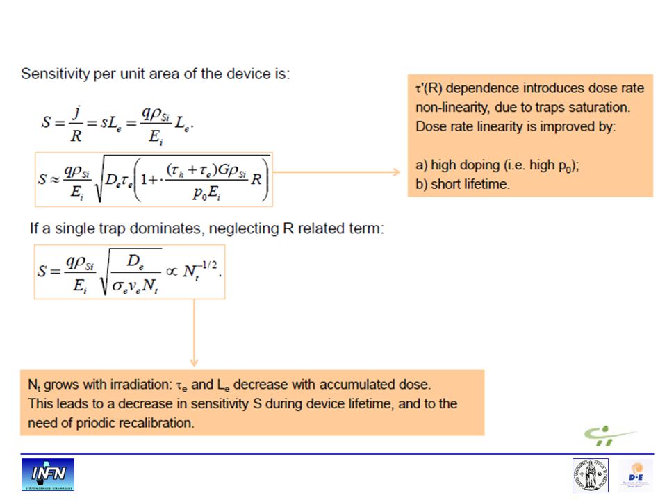
a) null bias; b) DC coupling; c) Sampling time and reset fixed by digital electronics (usually T≈10ms); d) Only integrated charge measured. 1.5Gy/min Sensitivity of the device scales with diffusion length: Si dosimeter working principle: Photovoltaic Mode Mara Bruzzi, Danno da radiazione in semiconduttori Scuola Nazionale rivelatori ed elettronica per fisica delle alte energie, astrofisica 12 Aprile 2011, Legnaro, Italy

97
Decrease in sensitivity with the accumulated dose due to the generation of a dominant trap acting as lifetime killer. 1/ - 1/ 0 = v th N t, N t = a ; a = trap generation rate capture cross section ; v th carrier thermal velocity. N t trap concentration. a DOFZ < a S FZ increased radiation hardness of the device to radiotherapic beams. Improved radiation hardness of DOFZ Si a DOFZ = 5.0x10 7 cm -3 Gy -1, a STFZ = 8.1x10 7 cm -3 Gy -1 Material engineering concepts have been applied also to Silicon dosimeters for radiotherapy M. Casati et al. NIM A 2005 Mara Bruzzi, Danno da radiazione in semiconduttori Scuola Nazionale rivelatori ed elettronica per fisica delle alte energie, astrofisica 12 Aprile 2011, Legnaro, Italy

98
First radiation hardness solution (≈1980) has been pre-irradiation before use. In fact, since S N t -1/2 pre-irradiation reduces the slope of sensitivity vs. dose curve. Usually 10kGy are adopted as a typical pre-irradiation. Radiation hardness of Si dosimeters Mara Bruzzi, Danno da radiazione in semiconduttori Scuola Nazionale rivelatori ed elettronica per fisica delle alte energie, astrofisica 12 Aprile 2011, Legnaro, Italy

99
Another radiation hardness solution (≈ 1980) was: working with p-type materials. In fact, dominant center produced by electron irradiation has cross sections: This means that for this center is easier to capture holes. As diffusion is ruled by minority carriers, to get a transport less influenced by irradiation minority carriers must be electrons, thus material has to be p-type. Mara Bruzzi, Danno da radiazione in semiconduttori Scuola Nazionale rivelatori ed elettronica per fisica delle alte energie, astrofisica 12 Aprile 2011, Legnaro, Italy

100
Material Engineering Recipe. Pt doping

101
Our recipe: Low resistivity epitaxial p-type Si on MCz substrates Concept: active region is limited in any direction to a value shorter than L e at the highest dose of interest. Epitaxial Layer is used to limit active depth, guard-ring to limit active area. Mara Bruzzi, Danno da radiazione in semiconduttori Scuola Nazionale rivelatori ed elettronica per fisica delle alte energie, astrofisica 12 Aprile 2011, Legnaro, Italy

102
Improved stability of the sensitivity with the accumulated dose by using epitaxial Si ( p-type ) with guard ring to confine the active volume of the device M. Bruzzi et al. App. Phys. Lett, 2007. Italian patent No. FI2006A000166 Mara Bruzzi, Danno da radiazione in semiconduttori Scuola Nazionale rivelatori ed elettronica per fisica delle alte energie, astrofisica 12 Aprile 2011, Legnaro, Italy

103
Main sources of radiation affecting PV modules are protons and electrons trapped by the terrestrial magnetic field and protons coming from the Sun, the particle flux depending on the orbit of the mission. Radiation damage in satellites at low altitude orbits (lower than 800 km) or in the high altitude ones (5000 km or higher) is mainly produced by protons (close to 90% of damage). Most advantageous orbits for a global satellite network, both from cost and operational viewpoints, may be in Medium Earth Orbits (MEO), in the 2000–10 000 km range. Unfortunately, these orbits are in the midst of the Van Allen radiation belts, where the severe radiation environment causes a rapid degradation of the solar cells. Further Example: Solar cells in space radiation levels Mara Bruzzi, Danno da radiazione in semiconduttori Scuola Nazionale rivelatori ed elettronica per fisica delle alte energie, astrofisica 12 Aprile 2011, Legnaro, Italy
 or in the high altitude ones (5000 km or higher) is mainly produced by protons (close to 90% of damage). Most advantageous orbits for a global satellite network, both from cost and operational viewpoints, may be in Medium Earth Orbits (MEO), in the 2000– km range. Unfortunately, these orbits are in the midst of the Van Allen radiation belts, where the severe radiation environment causes a rapid degradation of the solar cells. Further Example: Solar cells in space radiation levels Mara Bruzzi, Danno da radiazione in semiconduttori Scuola Nazionale rivelatori ed elettronica per fisica delle alte energie, astrofisica 12 Aprile 2011, Legnaro, Italy.")
104
Typical solar cell module is composed of n + /p/p + junctions made on Silicon, used in photovoltaic mode. The built-in electric field leads to the separation of the charge carriers that are released by light. Silicon cells are approximately 10 cm by 10 cm large (recently also 15 cm by 15 cm). A transparent anti-reflection film protects the cell and decreases reflective loss on the cell surface. /26 Working principle of a solar cell Mara Bruzzi, Danno da radiazione in semiconduttori Scuola Nazionale rivelatori ed elettronica per fisica delle alte energie, astrofisica 12 Aprile 2011, Legnaro, Italy
. A transparent anti-reflection film protects the cell and decreases reflective loss on the cell surface. /26 Working principle of a solar cell Mara Bruzzi, Danno da radiazione in semiconduttori Scuola Nazionale rivelatori ed elettronica per fisica delle alte energie, astrofisica 12 Aprile 2011, Legnaro, Italy.")
105
Solar cell efficiency factors Maximum-power point By increasing the resistive load on an irradiated cell continuously from zero (a short circuit) to a very high value (an open circuit) one can determine the maximum-power point, that is, the load for which the cell can deliver maximum electrical power at that level of irradiation. V m x I m = P m. Fill factor Another defining term in the overall behavior of a solar cell is the fill factor (FF). This is the ratio of the maximum power divided by the open circuit voltage (V oc ) and the short circuit current (I sc ): Energy conversion efficiency A solar cell's energy conversion efficiency (η), is the percentage of power converted from absorbed light to electrical energy, calculated as P m divided by the input light irradiance under "standard" test conditions (E, in W/m 2 ) and the surface area of the solar cell (A c in m²). /26 Mara Bruzzi, Danno da radiazione in semiconduttori Scuola Nazionale rivelatori ed elettronica per fisica delle alte energie, astrofisica 12 Aprile 2011, Legnaro, Italy
. This is the ratio of the maximum power divided by the open circuit voltage (V oc ) and the short circuit current (I sc ): Energy conversion efficiency A solar cell s energy conversion efficiency (η), is the percentage of power converted from absorbed light to electrical energy, calculated as P m divided by the input light irradiance under standard test conditions (E, in W/m 2 ) and the surface area of the solar cell (A c in m²). /26 Mara Bruzzi, Danno da radiazione in semiconduttori Scuola Nazionale rivelatori ed elettronica per fisica delle alte energie, astrofisica 12 Aprile 2011, Legnaro, Italy.")
106
Deterioration of operative parameters of the solar cell due to the change of minority carrier lifetime Radiation Damage in Si Solar cells Mara Bruzzi, Danno da radiazione in semiconduttori Scuola Nazionale rivelatori ed elettronica per fisica delle alte energie, astrofisica 12 Aprile 2011, Legnaro, Italy

107
Conclusions Microscopic view of radiation Damage is a useful tool to quantitatively explain macroscopic radiation damage in semiconductor devices Material/Device Enginering successful Best to work on the subject interdisciplinarly RD50 forum for development of Ultra Radiation Hard Semiconductor Detectors Mara Bruzzi, Danno da radiazione in semiconduttori Scuola Nazionale rivelatori ed elettronica per fisica delle alte energie, astrofisica 12 Aprile 2011, Legnaro, Italy

108
Mara Bruzzi, Danno da radiazione in semiconduttori Scuola Nazionale rivelatori ed elettronica per fisica delle alte energie, astrofisica 12 Aprile 2011, Legnaro, Italy

109
Le proprieta’ dosimetriche dopo irraggiamento con neutroni migliorano drasticamente a causa della rimozione di livelli energetici profondi M. Bruzzi et al. App.Phys.Lett. (2002) L’irraggiamento con elevate fluenze può anche migliorare le prestazioni del dispositivo: per esempio questo avviene nel dosimetro al diamante
 L’irraggiamento con elevate fluenze può anche migliorare le prestazioni del dispositivo: per esempio questo avviene nel dosimetro al diamante.")
110
Forte diminuzione dei segnali TSC e PICTS relativi ai difetti responsabili della instabilità di corrente dopo irraggiamento con neutroni a tale fluenza

111
SiC: not radiation resistant as a high energy physics detector and a radiotherapy dosimeter. [F. Nava, INFN & University of Modena, Oct. 2004]

112
But good radiation resistance as UV photodetector, extremely stable for long periods of time even when exposed to high doses of UV radiation of up to 100W/m²

113
Mara Bruzzi, April 11, 2011 Thermodinamically, the ionization energy E t is defined as the chemical potential for the reaction forming one ionized defect and a free carrier. This is equal to the increase in the Gibbs free energy upon increasing the number of free carriers by one at constant temperature and pressure: t = H t -T S t The capture cross section is also temperature dependent according to the law: and: Where the entropy term is included in na (apparent cross section) and E na represent the activation energy of the trap (electrons). Activation energy and apparent cross section
 and E na represent the activation energy of the trap (electrons). Activation energy and apparent cross section.")
Presentazioni simili


 SEZIONI INFN COINVOLTE: +FI.>")


>")

>")


